Semiconductor memory device
a memory device and semiconductor technology, applied in semiconductor devices, digital storage, instruments, etc., can solve the problems of reducing the thickness of the gate oxide, the current drivability cannot be increased, and the swing voltage of the word line cannot be lowered, so as to improve the access time and cycle time, the time for reading memory cell data to the bit line increases, and the current drivability is reduced
- Summary
- Abstract
- Description
- Claims
- Application Information
AI Technical Summary
Benefits of technology
Problems solved by technology
Method used
Image
Examples
embodiment 1
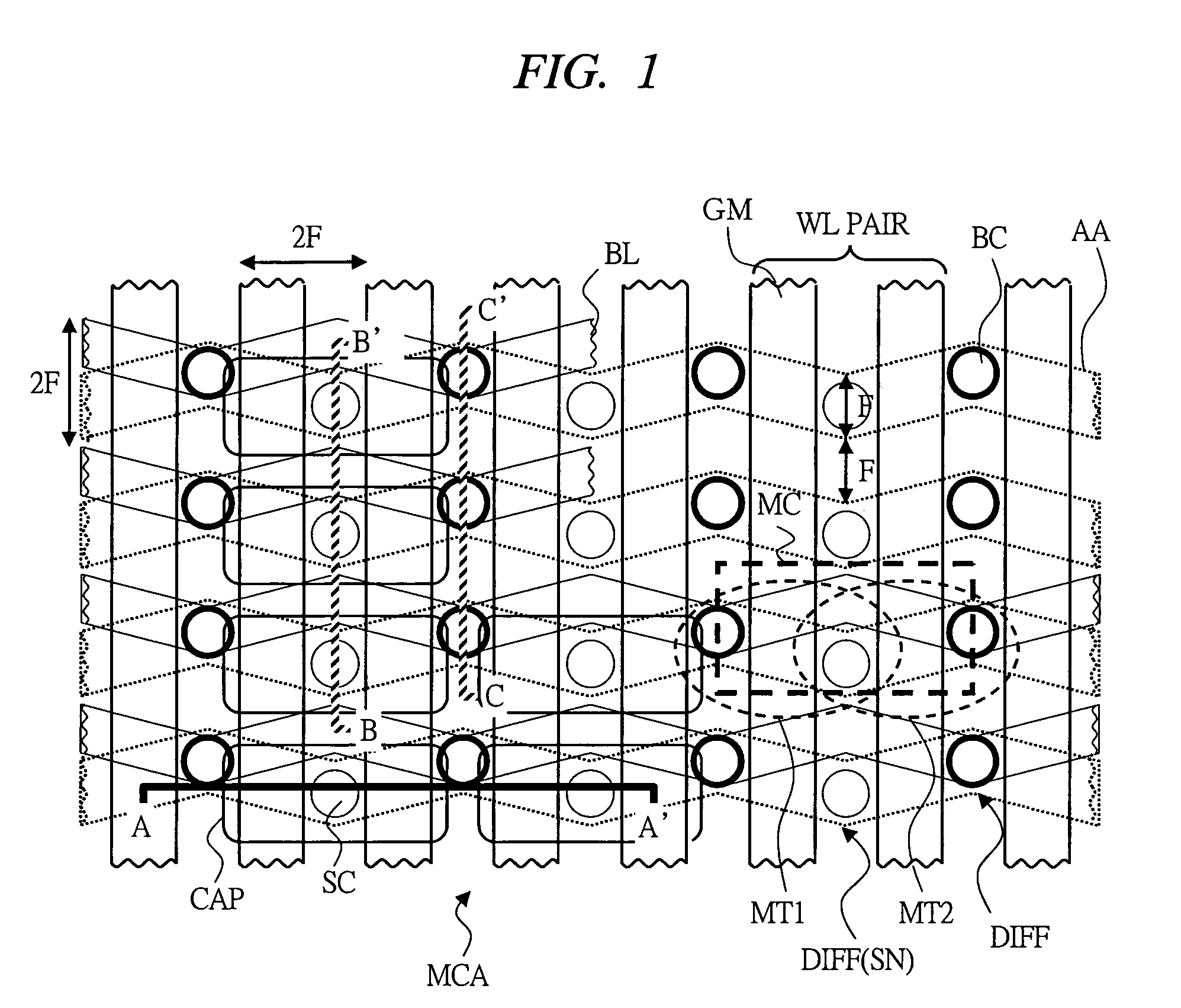
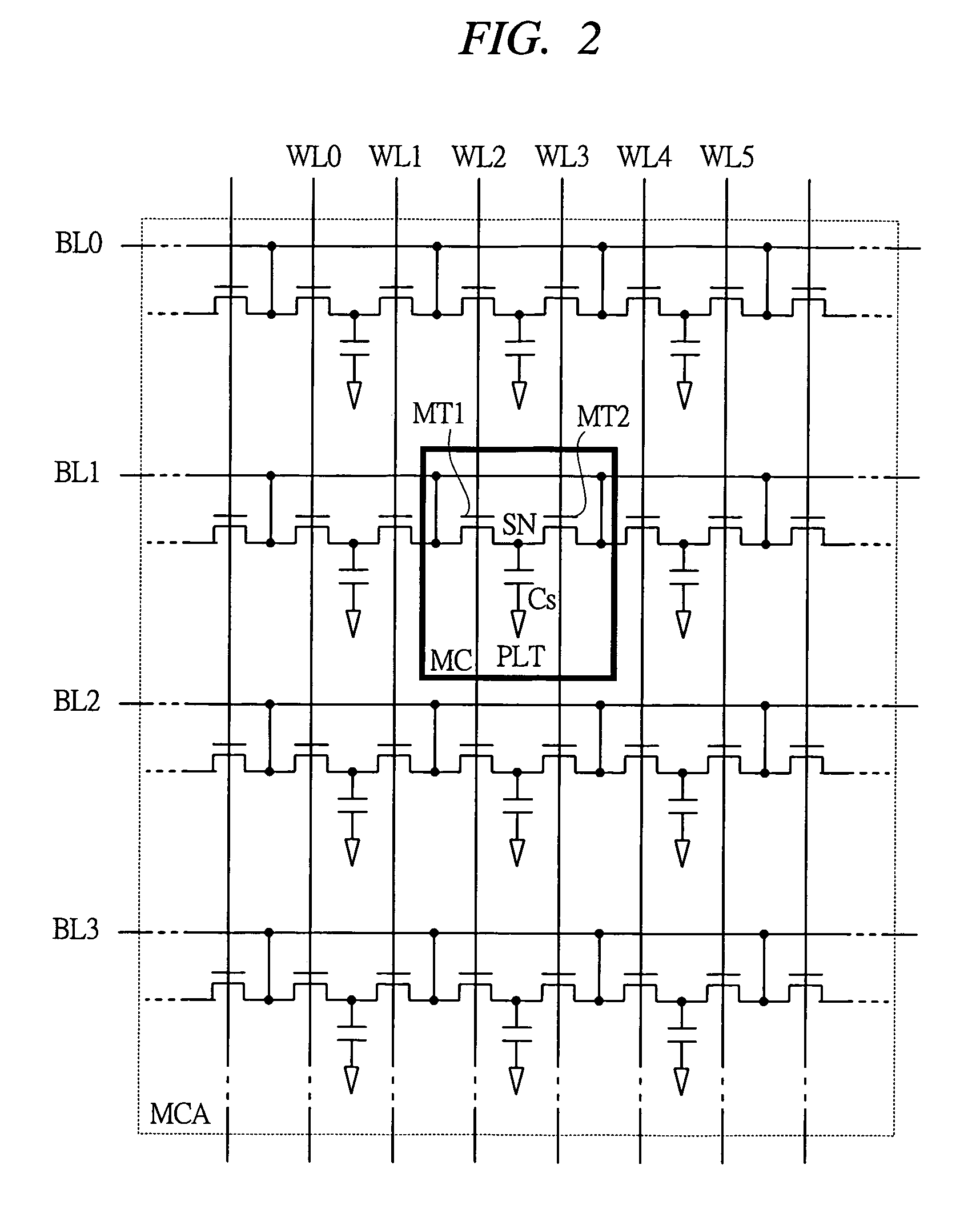
[0059]FIG. 1 is a layout drawing showing one example of the memory cell layout in a semiconductor memory device according to embodiment 1 of the present invention. FIG. 2 is an equivalent circuit diagram that corresponds to the memory cell layout of FIG. 1.
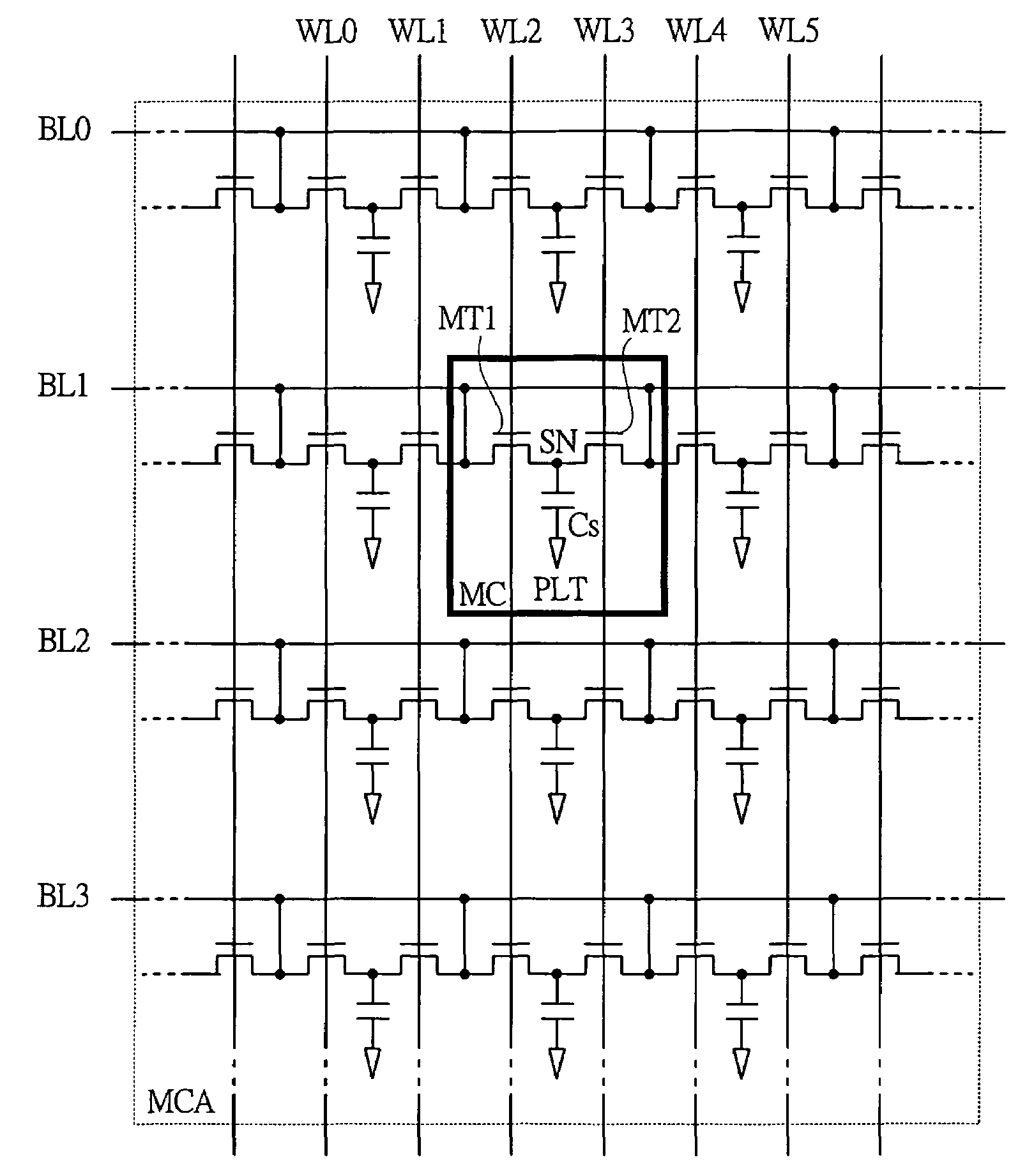
[0060]As illustrated in FIG. 2, the semiconductor memory device according to embodiment 1 of the present invention has a memory cell MC at a desired intersection between a word line WL and a bit line BL in a memory cell array MCA, and one memory cell MC comprises two memory cell transistors MT1, MT2 and one capacitor Cs to store information as electric charges. In the memory cell MC, to a storage node SN (first node), one ends of source terminal / drain terminal of two memory cell transistors MT1, MT2 and one end of capacitor Cs are connected in common, and to bit line BL1, the other ends (second node) of memory cell transistors MT1, MT2 are independently connected, respectively.
[0061]Let the wiring pitch of word line WL be 2F (F: f...
embodiment 2
[0090]FIG. 3 is a layout drawing showing one example of the memory cell layout in a semiconductor memory device according to embodiment 2 of the present invention. The memory cell layout shown in FIG. 3 differs from FIG. 1 described above and is characterized in that the bit line and wiring patterns of the diffusion layer row are wired to achieve waveforms of 8F cycle.
[0091]The bit line contact BC is disposed at the portion where the bit line BL and the diffusion layer row (active region AA) intersect, and the storage node contact SC is disposed at the position where the bit line BL and the diffusion layer row do not overlap in the perpendicular line but is disposed at the position shifted just by F. The storage node contact SC of the memory cell MC connected to the bit line BL is disposed alternately top and bottom with respect to the bit line BL. Because this arrangement can make the wave-form cycle of the bit line BL and diffusion layer row become 8F as described above as well as...
embodiment 3
[0097]FIG. 4 is a layout drawing showing one example of the memory cell layout in a semiconductor memory device according to embodiment 3 of the present invention. The memory cell layout shown in FIG. 4 differs from cases of embodiments 1, 2 and bit lines and diffusion layer row are disposed perfectly parallel in the vertical direction, and is a suitable layout in which the capacitor is formed below the bit line wiring layer.
[0098]According to this kind of layout, since the bit lines and diffusion layer row are disposed completely in parallel in the vertical direction, processing and formation of bit lines and diffusion layer row become easy. In addition, because same as the cases of embodiments 1, 2 described above, the width of the diffusion layer region which is the gate width of memory cell transistor becomes F, the total gate width of the memory cell transistors connected between one memory cell capacitor and the bit line becomes 2F. The area of memory cell MC in this event is ...
PUM
 Abstract
Description
Claims
Application Information


