Semiconductor device having buried gate structure and method for fabricating the same

a semiconductor device and gate structure technology, applied in the direction of semiconductor devices, electrical appliances, basic electric elements, etc., can solve the problems affecting the performance of the buried gate-type transistor, and achieve the effect of reducing the leakage of gate-induced drain and improving the refresh characteristics

Active Publication Date: 2018-06-21
SK HYNIX INC
View PDF0 Cites 27 Cited by
  • Summary
  • Abstract
  • Description
  • Claims
  • Application Information

AI Technical Summary

Benefits of technology

[0005]Embodiments of the present invention are directed to a semiconductor device capable of reducing a gate-induced drain leakage (GIDL), and a method for fabricating the semiconductor device.
[0006]Embodiments of the present invention are directed to a memory cell exhibiting improved refresh characteristics.

Problems solved by technology

Also, gate-induced drain leakage (GIDL) characteristics may affect the performance of the buried gate-type transistor.

Method used


Image

  • Semiconductor device having buried gate structure and method for fabricating the same
  • Semiconductor device having buried gate structure and method for fabricating the same
  • Semiconductor device having buried gate structure and method for fabricating the same

Examples


first embodiment

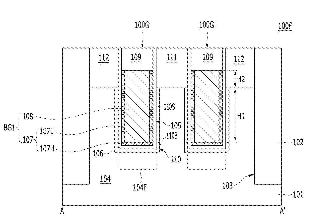
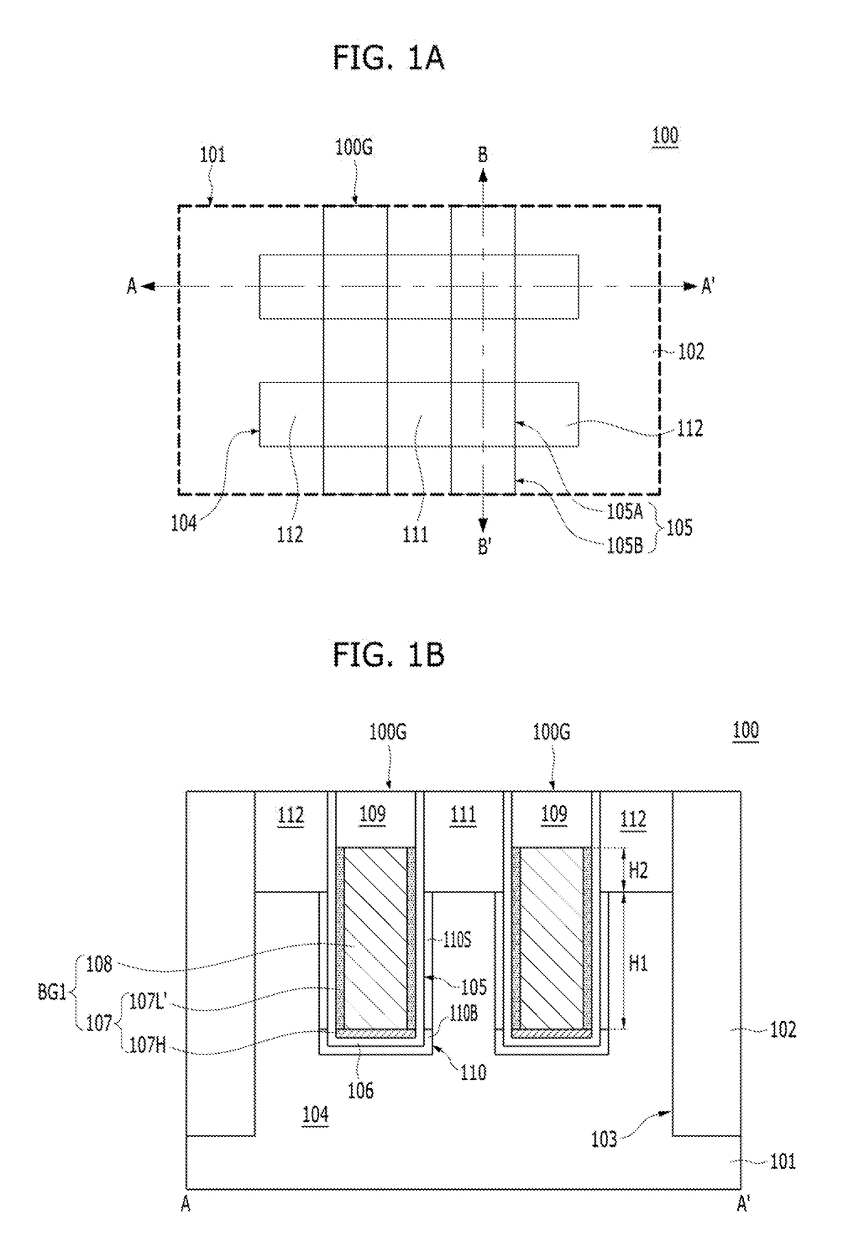
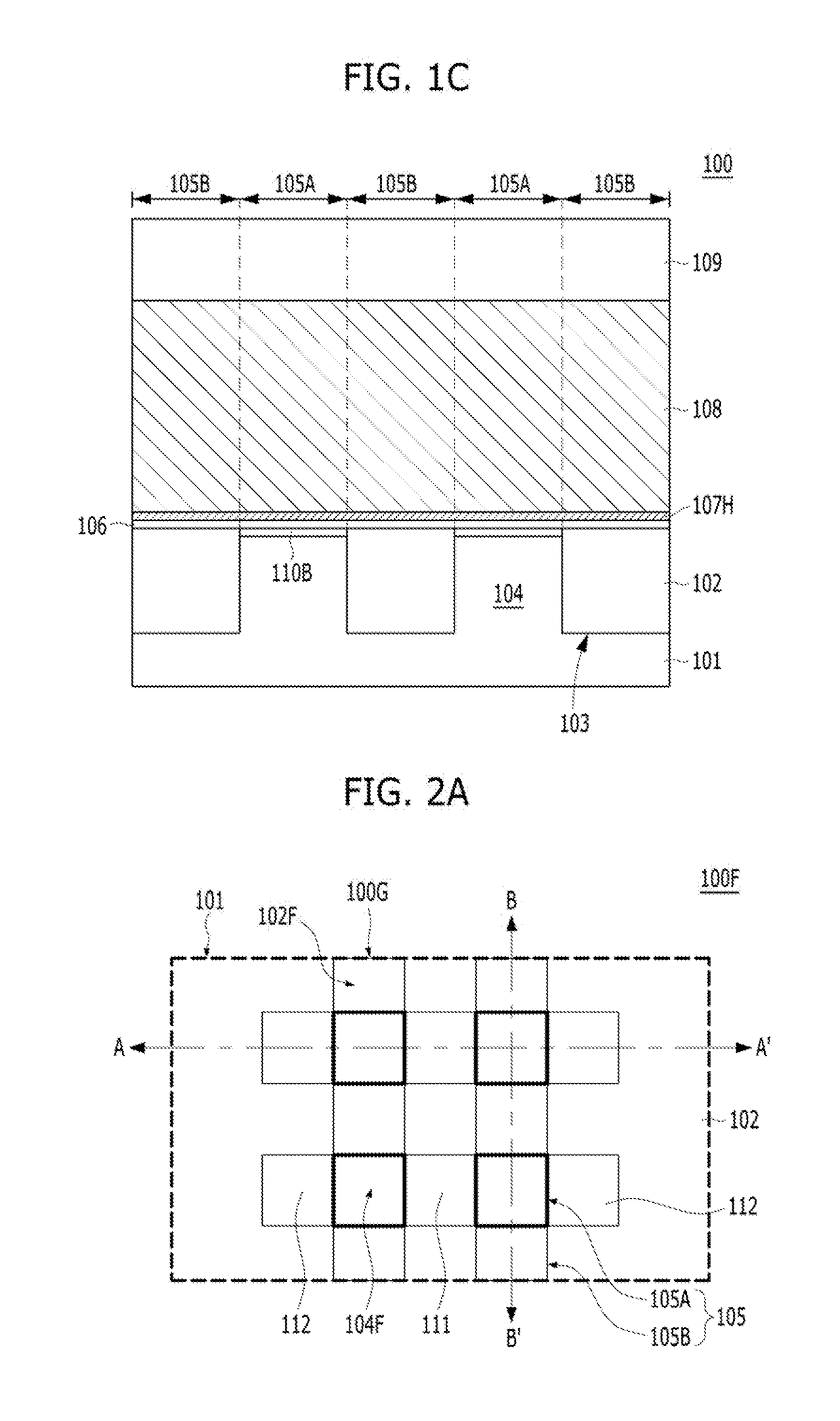
[0061]FIG. 1A is a plan view illustrating a semiconductor device in accordance with the present invention. FIG. 1B is a cross-sectional view of the semiconductor device of FIG. 1A taken along a line A-A′. FIG. 1C is a cross-sectional view of the semiconductor device of FIG. 1A taken along a line B-B′.

[0062]Referring to FIGS. 1A to 1C, a semiconductor device 100 in accordance with an embodiment of the present invention may include a transistor.

[0063]The semiconductor device 100 may include a substrate 101, a gate trench 105, a channel region 110, a buried gate structure 100G, a first doped region 111, and a second doped region 112. The buried gate structure 100G may include a gate dielectric layer 106, a buried gate electrode BG1, and a capping layer 109. The buried gate electrode BG1 may include a work function layer 107, and a gate conductive layer 108. The work function layer 107 may include an undoped high work function layer 107H and a doped low work function layer 107L′.

[0064]T...

third embodiment

[0097]Referring to FIG. 3A, some constituents of the semiconductor device 200 in accordance with the present invention may be the same as those of the semiconductor device 100. The semiconductor device 200 may include a substrate 101, an isolation layer 102, an active region 104, a gate trench 105, a channel region 110, a buried gate structure 200G, a first doped region 111, and a second doped region 112. The buried gate structure 200G may include a gate dielectric layer 106, a buried gate electrode BG2, and a capping layer 109. The buried gate electrode BG2 may include a work function layer 207, and a gate conductive layer 108. The channel region 110 may include a bottom channel 110B and a side channel 110S.

[0098]The work function layer 207 may be made of a metal nitride. The work function layer 207 may include a titanium nitride (TiN), a titanium aluminum nitride (TiAlN), or a titanium aluminum (TiAl).

[0099]The work function layer 207 may locally contain a work function adjustment...

fifth embodiment

[0116]Referring to FIG. 5A, some constituents of the semiconductor device 400 in accordance with the present invention may be the same as those of the semiconductor device 100. The semiconductor device 400 may include a substrate 101, an isolation layer 102, an active region 104, a gate trench 105, a channel region 110, a buried gate structure 400G, a first doped region 111, and a second doped region 112. The buried gate structure 400G may include a gate dielectric layer 106, a buried gate electrode BG4, and a capping layer 109. The buried gate electrode BG4 may include a work function layer 407, a gate conductive layer 108, a barrier layer 113, and a silicon-based low work function layer 114. The work function layer 407 may include an undoped high work function layer 107H and a doped low work function layer 107L′. The channel region 110 may include a bottom channel 110B and a side channel 110S.

[0117]The undoped high work function layer 107H may include an undoped titanium nitride. ...


PUM


Abstract

A method for fabricating a semiconductor device includes: forming a gate trench in a semiconductor substrate; forming a gate dielectric layer over a bottom surface and sidewalls of the gate trench; forming a first work function layer over the gate dielectric layer; doping a work function adjustment element to form a second work function layer which overlaps with the sidewalls of the gate trench; forming a gate conductive layer that partially fills the gate trench; and forming doped regions inside the semiconductor substrate on both sides of the gate trench.

Description

CROSS-REFERENCE TO RELATED APPLICATIONS[0001]The present application claims priority of Korean Patent Application No. 10-2016-0172646, filed on Dec. 16, 2016, which is incorporated herein by reference in its entirety.BACKGROUND1. Field[0002]Exemplary embodiments of the present invention relate to a semiconductor device having a buried gate structure, a method for fabricating the semiconductor device, and a memory cell including the semiconductor device.2. Description of the Related Art[0003]A metal gate electrode is used for a high-performance transistor. In particular, a threshold voltage needs to be controlled for a high-performance operation of a buried gate-type transistor. Also, gate-induced drain leakage (GIDL) characteristics may affect the performance of the buried gate-type transistor.SUMMARY[0004]Embodiments of the present invention are directed to a buried gate structure capable of shifting a threshold voltage, and a method for fabricating the buried gate structure.[0005]...

Claims


Application Information

Patent Timeline
Patent Type & Authority Applications(United States)
IPC IPC(8): H01L21/28H01L29/423H01L29/49H01L29/66H01L29/78
CPCH01L21/28088H01L29/4236H01L29/4966H01L29/66666H01L29/7827H01L27/10805H01L27/228H01L27/2454H01L21/28H01L29/10H01L21/26586H01L29/66621H01L29/78H01L21/28114H10B63/34H10B61/22H10N50/01H10N70/231H10N70/20H10N70/8825H10N70/8828H10N70/8833H10N70/011H10B12/038H01L29/42356H01L29/6656H01L29/4234H01L29/42324H01L21/02068H01L21/76829H01L29/36H10B12/30
Inventor JANG, TAE-SUPARK, JIN-CHULPARK, JI-HWANJANG, IL-SIKRYU, SEONG-WANKWON, SE-INSHIN, JUNG-HOHAM, DAE-JIN
Owner SK HYNIX INC
Why Eureka
Try Eureka