Chip parts and method for manufacturing the same, circuit assembly having the chip parts and electronic device

a technology of chip parts and circuit parts, which is applied in the direction of fixed capacitor details, electrical apparatus casings/cabinets/drawers, stacked capacitors, etc., can solve problems such as restrictions, and achieve the effect of smooth mounting and preventing the chip part from slipping off the mounting substra

Active Publication Date: 2015-07-30
ROHM CO LTD
View PDF7 Cites 13 Cited by
  • Summary
  • Abstract
  • Description
  • Claims
  • Application Information

AI Technical Summary

Benefits of technology

[0007]Although the problem may be solved by changing a condition (specification) of the light source which is disposed in the peripheries of the part recognizing camera, there is a fear that some restrictions may arise, for example, the same automatic mounting machine may not be used in a chip part different in specification. As a result, smooth mounting of the chip part is prevented by occurrence of misrecognition by the automatic mounting machine.
[0008]A preferred embodiment of the present invention is to provide a chip part which can be determined satisfactorily for a front surface or a rear surface thereof and mounted smoothly on a mounting substrate and also to provide a method for manufacturing thereof.

Problems solved by technology

However, the chip part is not always suctioned by the suction nozzle horizontally but may be suctioned by the suction nozzle in an inclined manner from time to time.
Although the problem may be solved by changing a condition (specification) of the light source which is disposed in the peripheries of the part recognizing camera, there is a fear that some restrictions may arise, for example, the same automatic mounting machine may not be used in a chip part different in specification.

Method used


Image

  • Chip parts and method for manufacturing the same, circuit assembly having the chip parts and electronic device
  • Chip parts and method for manufacturing the same, circuit assembly having the chip parts and electronic device
  • Chip parts and method for manufacturing the same, circuit assembly having the chip parts and electronic device

Examples


modification examples

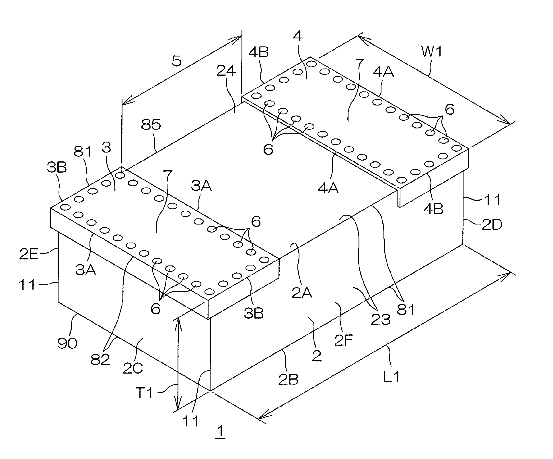
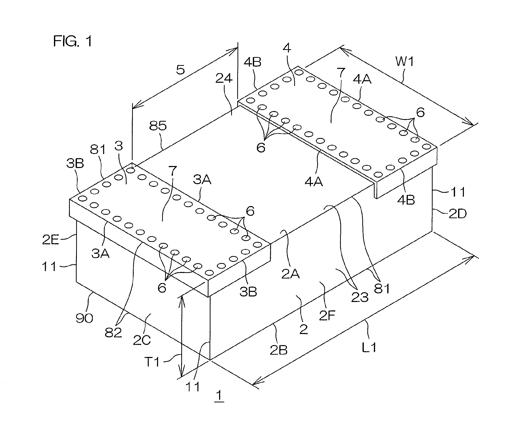
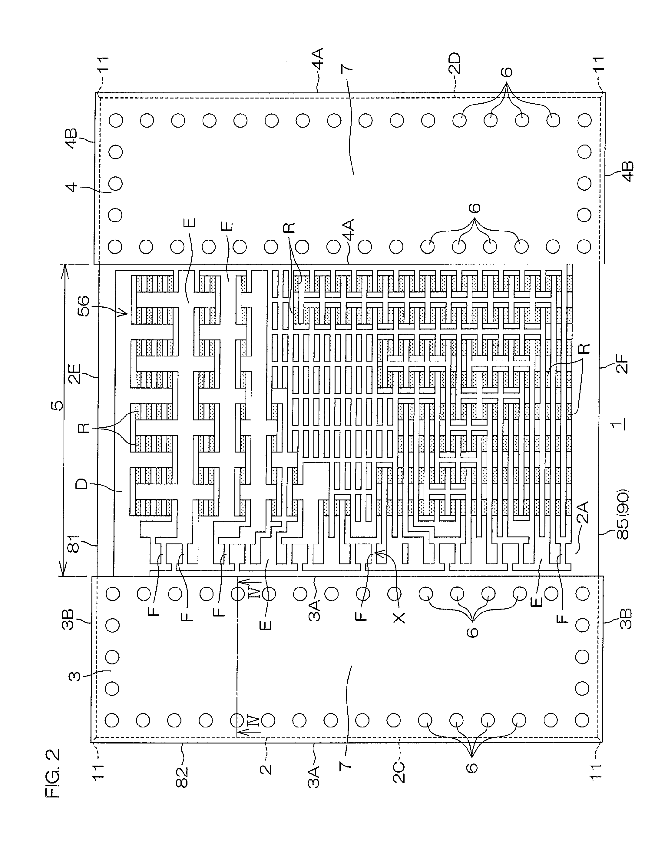
[0578]Although in Embodiment 1 to Embodiment 5, the insulating film 20 is formed on the front surface of the substrate 2, an arrangement shown inFIG. 66 may be adopted. FIG. 66 is a schematic sectional view which shows a first connection electrode 3 of a chip part 701 according to a modification example.

[0579]The chip part 701 of the modification example is different from the chip part 1 of Embodiment 1 in that an insulating substrate 702 made of an insulating material is formed, an insulating film 20 is not formed, and a base recessed portion 708 is formed on a front surface of the insulating substrate 702. In FIG. 66, for the sake of explanation, the chip part is shown as a modification example of Embodiment 1. However, the chip part is also applicable to each arrangement of Embodiment 2 to Embodiment 5. In FIG. 66, the portions corresponding to the individual portions shown in FIG. 1 to FIG. 65 are given the same reference numerals, with a description thereof omitted.

[0580]The in...


PUM


Abstract

The chip part of the present invention includes a substrate, an electrode on the substrate and having a front surface in which a plurality of recessed portions are formed toward the thickness direction thereof, and an element region having a circuit element that is electrically connected to the electrode.

Description

CROSS-REFERENCE TO RELATED APPLICATIONS[0001]The present application corresponds to Japanese Patent Application No. 2013-272825 filed in the Japan Patent Office on Dec. 27, 2013, Japanese Patent Application No. 2013-272826 filed in the Japan Patent Office on Dec. 27, 2013, and Japanese Patent Application No. 2014-225234 filed in the Japan Patent Office on Nov. 5, 2014, and all the disclosures of the applications will be incorporated herein by citation.FIELD OF THE INVENTION[0002]The present invention relates to a chip part, a method for manufacturing the chip part, and a circuit assembly and an electronic device which include the chip part.BACKGROUND ART[0003]Patent Document 1 (Japanese Patent Application Publication No. 2001-76912) has disclosed a chip resistor in which an electrode is formed on a surface at one side of an insulating substrate. This chip resistor is soldered onto a mounting substrate, with the surface at one side faced downward.BRIEF SUMMARY OF THE INVENTION[0004]I...

Claims


Application Information

Patent Timeline
Patent Type & Authority Applications(United States)
IPC IPC(8): H05K1/02H05K3/00H05K1/09H05K5/00H05K1/11
CPCH05K1/0296H05K5/0091H05K3/0011H05K1/09H05K1/11H01L27/016H01C1/14H01C1/142H01C7/003H01C7/006H01C17/006H01G4/012H01G4/30H01G4/33H01L27/0802H01L27/0805H01L28/20H01L28/60H05K1/167Y10T29/49158
Inventor TAMAGAWA, HIROSHIKONDO, YASUHIROYAMAMOTO, HIROKI
Owner ROHM CO LTD
Why Eureka
Try Eureka