Isolation methods for leakage, loss and non-linearity mitigation in radio-frequency integrated circuits on high-resistivity silicon-on-insulator substrates

a radio-frequency integrated circuit and substrate technology, applied in the field of electronics, can solve the problems of reducing the overall resistivity of the bulk substrate, adversely affecting transistor performance, increasing the capacitive coupling in the soi substrate, etc., to reduce the non-linear effect of rf signals, reduce the coupling on rf transmission lines and losses, and reduce the cost

Inactive Publication Date: 2015-08-13
SKYWORKS SOLUTIONS INC
View PDF8 Cites 17 Cited by
  • Summary
  • Abstract
  • Description
  • Claims
  • Application Information

AI Technical Summary

Benefits of technology

This patent describes methods for improving performance and efficiency of electronic components called transistors by preventing unwanted electrical current from affecting their operation. These improvements can be achieved even when using lower cost materials that are commonly available today. By controlling these factors, researchers hope to create better performing electronics more affordably than before.

Problems solved by technology

The technical problem addressed in this patent relates to how to prevent unwanted coupling between certain parts of a semiconductor device caused by a phenomenon called parasitic surface conductance (PSC), while still maintaining the benefits of using high-resistivity silicon wafers to improve resistance and decrease loss. Various techniques exist to address this issue, including adding extra layers to the structure or developing specialized process technology, but they come with their own set of challenges and limitations.

Method used


Image

  • Isolation methods for leakage, loss and non-linearity mitigation in radio-frequency integrated circuits on high-resistivity silicon-on-insulator substrates
  • Isolation methods for leakage, loss and non-linearity mitigation in radio-frequency integrated circuits on high-resistivity silicon-on-insulator substrates
  • Isolation methods for leakage, loss and non-linearity mitigation in radio-frequency integrated circuits on high-resistivity silicon-on-insulator substrates

Examples


Embodiment Construction

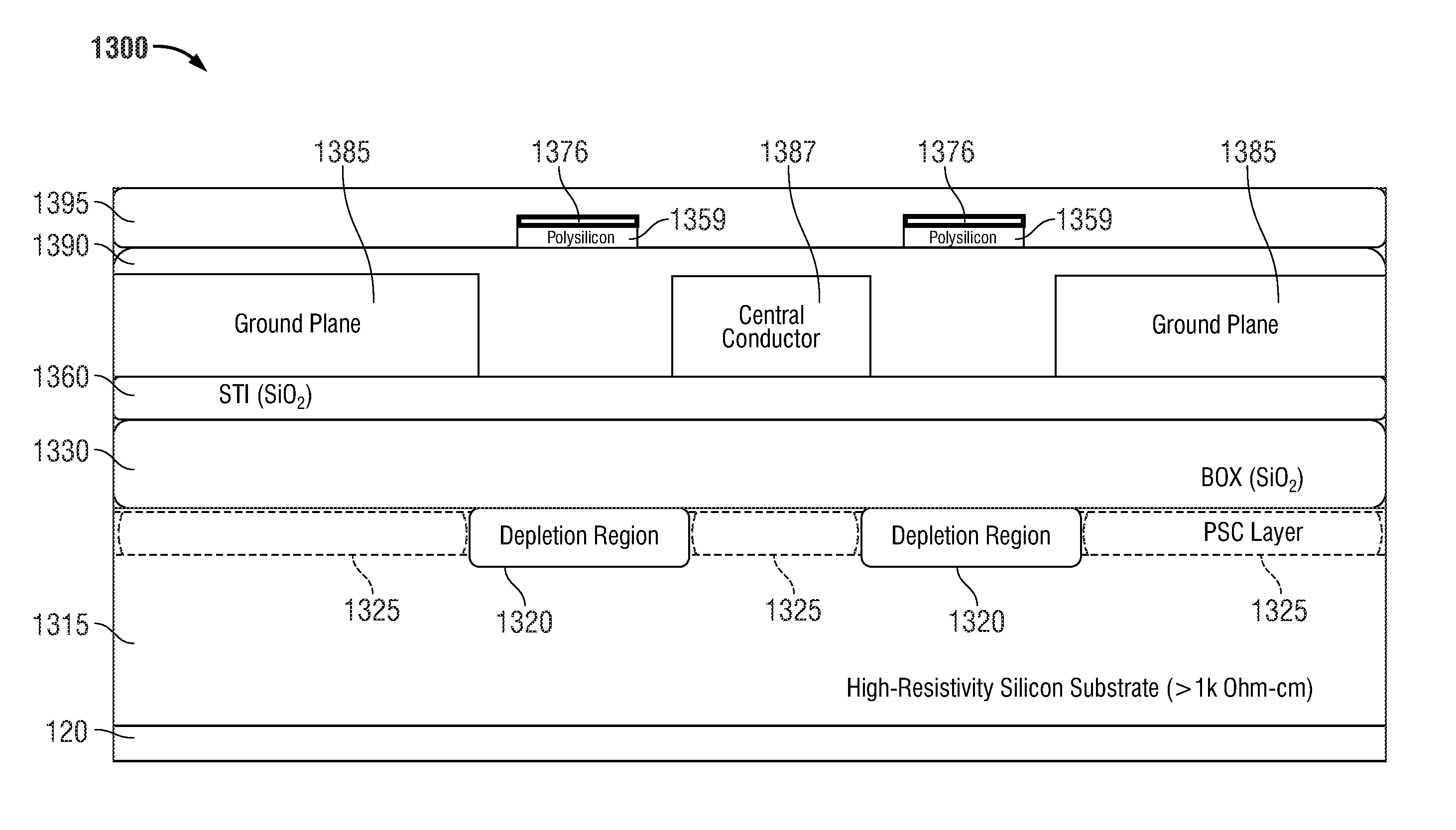
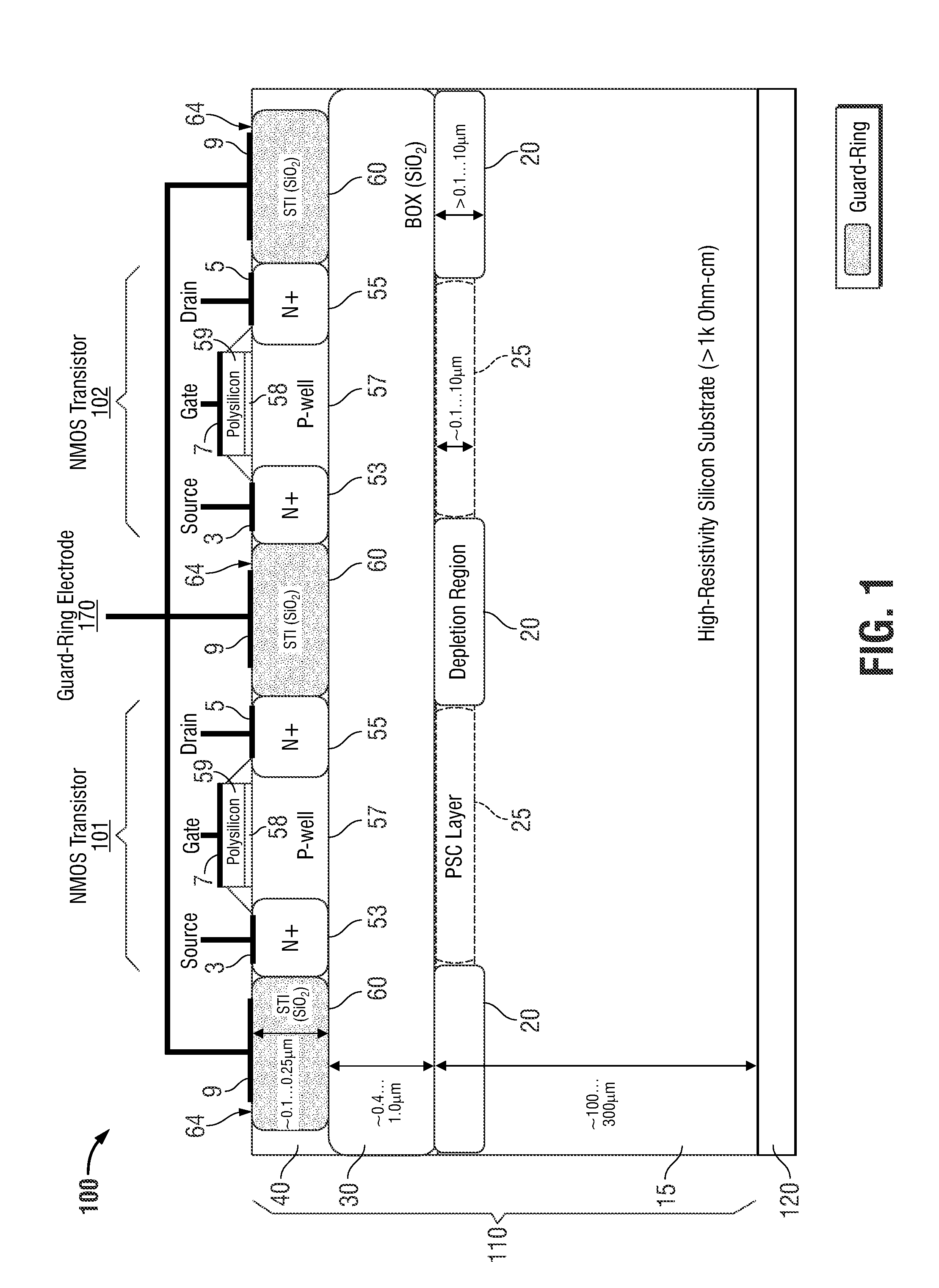
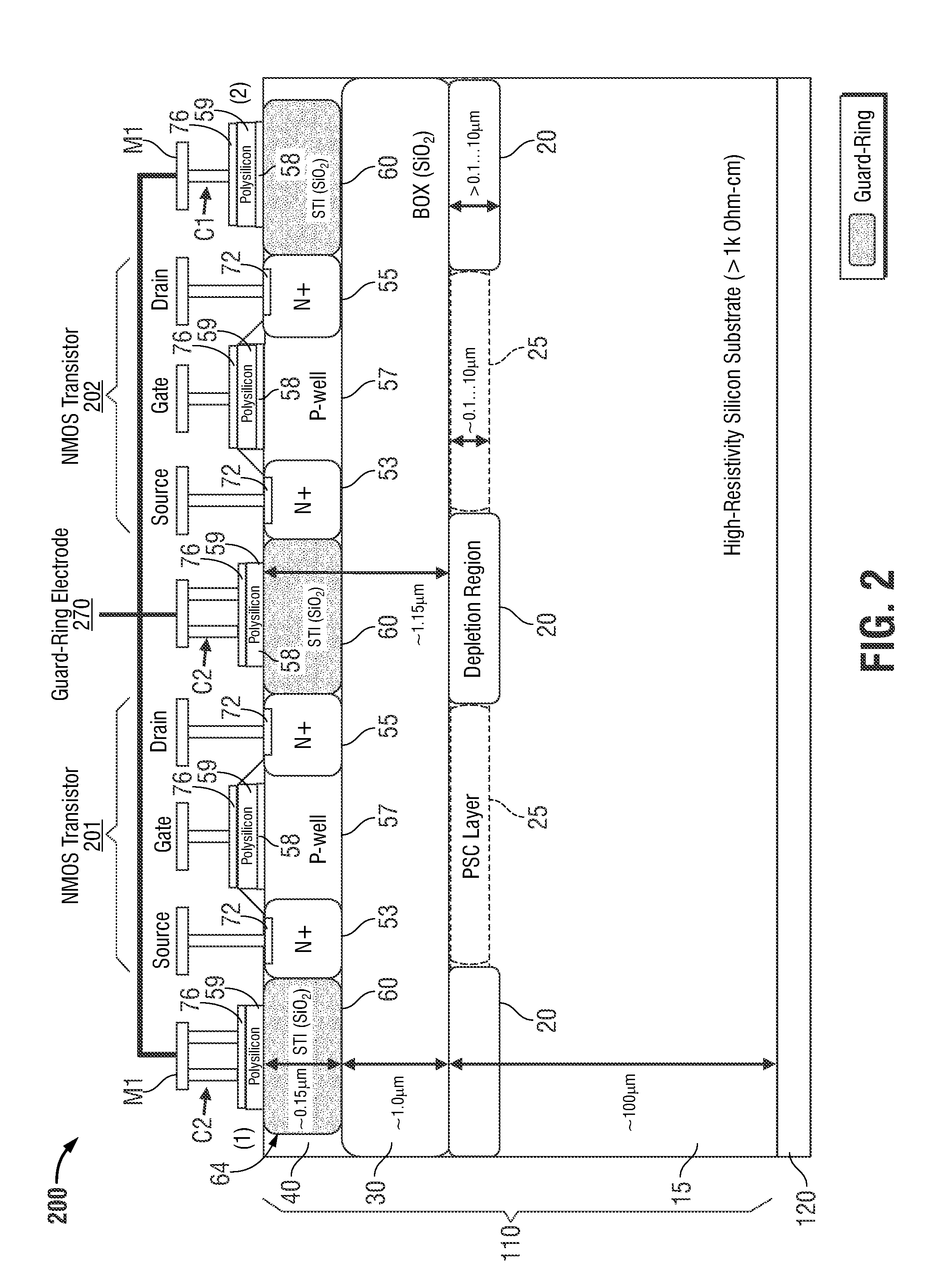
[0032]Hereinafter, embodiments of structures for implementing radio-frequency integrated circuits (RFICs) on high-resistivity silicon-on-insulator (SOI) substrates thereof, and methods of limiting a PSC layer in a RFIC, are described with reference to the accompanying drawings. Like reference numerals may refer to similar or identical elements throughout the description of the figures. It is understood that the following disclosure provides many different embodiments, or examples, for implementing different features of the invention. Specific examples of components and arrangements are described below to simplify the present disclosure. Many of the processes are known to one of skill in the art and are described in general detail only.

[0033]As it is used herein, the term ohms-cm (“ohms centimeter”) generally refers to the measurement of the volume resistivity (also known as bulk resistivity) of a semiconductor material. As used herein, “SOI transistors” generally refers to transisto...


PUM


Abstract

A radio frequency integrated circuit with a silicon-on-insulator substrate includes a buried oxide layer that is disposed over a silicon substrate. The silicon-on-insulator substrate has a silicon layer that is disposed over the buried oxide layer. The integrated circuit includes a transistor disposed on the silicon layer, and a guard-ring in the silicon-on-insulator substrate that surrounds the transistor on the silicon layer. Depletion regions on the silicon substrate corresponding to areas surrounding the transistor is defined by the application of a voltage to the guard-ring. Isolation of radio frequency transmission lines on silicon-on-insulator substrates is also possible with this configuration.

Description


Claims


Application Information

Patent Timeline
Owner SKYWORKS SOLUTIONS INC
Why Eureka
Try Eureka