

Methods for Wafer Bonding, and for Nucleating Bonding Nanophases
a technology of nanophases and nano-phases, which is applied in the direction of solid-state devices, semiconductor devices, basic electric elements, etc., can solve problems such as internal stresses and bonding failures
- Summary
- Abstract
- Description
- Claims
- Application Information
AI Technical Summary
Problems solved by technology
Method used
Image

Examples
example 1
Wafer Cleaning and Intermediate Processing
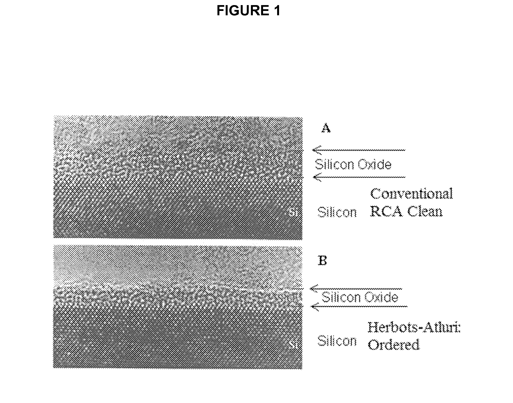
[0111]An innovative wet chemical clean and passivation for Si(100) wafers was developed in previous research by Atluri and Herbots et al. (see, U.S. Pat. No. 6,613,677). This process is unique in that it produces an ultra-flat (1×1) Si(100) ordered surface with extremely low surface impurity contamination compared to the well-known RCA type wet chemical cleans.
[0112]After cleaning, the optional intermediate processing of the wafers prior to bonding include packing the cleaned wafers in polypropylene or fluoropolymer containers under dry nitrogen and sealed in plastic bags filled with dry nitrogen. Wafers were stored in their sealed containers under dry nitrogen for up to a year before thermal processing. Wafers can be stored under dry nitrogen for 30 minutes to 3 days prior to thermal processing, or even longer. Wafers stored for over a year in sealed containers under dry nitrogen showed no evidence of an increase in surface contamination (e...
example 2
[0113]Low temperature (25° C.-200° C.) bonding between Si(100) and oxide wafers, either made of silica or oxidized Si(100) is achieved through a dual wet chemical process which terminates the stabilized ordered (1×1) Siwafer surface in air at room temperature with 2-D Langmuir-Blodgett film comprising of ordered arrays of —OH silanol groups (O2H2(1×1) Si(100)). The parallel wet chemical processing of the other oxide wafer surfaces in the bonding pair renders the SiO2 substoichiometric in oxygen and therefore hydrophilic with a net surface polarization, which can even result in a macroscopically observable net negative charge. If the surface of the O2H2(1×1) Si(100) is ordered, the net charge is very significant and the attractive force between it and other wafers sufficient to overcome the force of gravity to lift directly a wafer underneath for a distance of an inch to a cm or less. The overcoming of the force of gravity between the top wafer and the lower wafer to be bonded when p...
example 3
Electrical Nanobonding
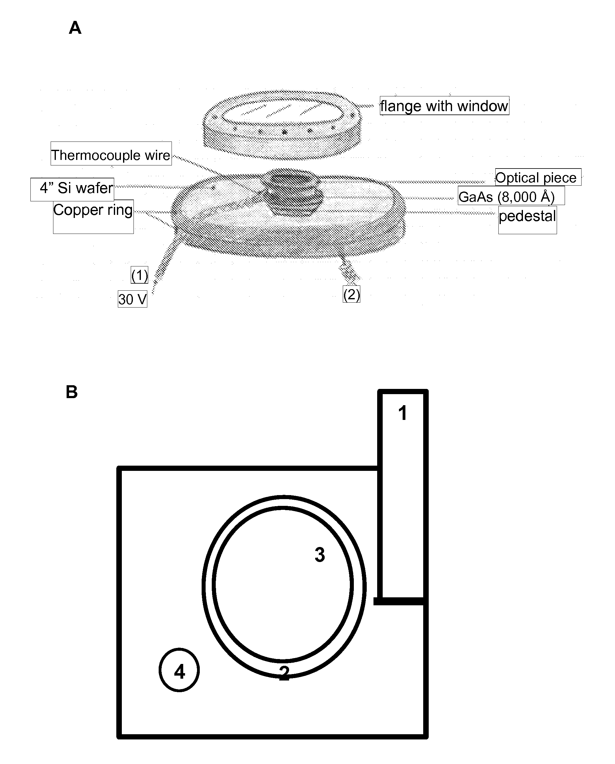
[0141]Electrostatic repulsion may be present between two surfaces that will be bonded. In a specific case, it is desired that optical glass will be bonded with GaAS with a SiO2 interface. The application of a polarization mechanism, such as plasma etching or sputtering with gas such as argon, results in a modification of the physical property of the materials due to embedded ions at the or below the surface of the material. The etching will alter the electrostatic interaction between the two substrates.
[0142]The surface of the GaAs wafer with the SiO2 interface is cleaned and prepared using the Herbots-Atluri method. In addition to the removal of particles from the surface, an ordered passivating layer of oxygen and hydrogen is formed on the substrate surface. Methods for preparing semiconductor substrates and interfacial oxides thereon, are also described in U.S. Pat. No. 7,851,365. Similarly, the optical glass can be cleaned and prepared using the Herbots-Atl...
PUM
 Abstract
Description
Claims
Application Information