Processes and Apparatus for Preparing Heterostructures with Reduced Strain by Radial Distension

a technology of radial distension and heterostructure, which is applied in the field of preparation of semiconductor heterostructures with reduced strain, can solve the problems of reducing the quality and usefulness of multi-layer semiconductor structures, straining of layers,

Active Publication Date: 2014-07-03
GLOBALWAFERS CO LTD
View PDF18 Cites 166 Cited by
  • Summary
  • Abstract
  • Description
  • Claims
  • Application Information

AI Technical Summary

Problems solved by technology

The lattice mismatch between layers causes the layers to be strained.
Such dislocations degrade the quality and usefulness of the multi-layer semiconductor structure.

Method used


Image

  • Processes and Apparatus for Preparing Heterostructures with Reduced Strain by Radial Distension
  • Processes and Apparatus for Preparing Heterostructures with Reduced Strain by Radial Distension
  • Processes and Apparatus for Preparing Heterostructures with Reduced Strain by Radial Distension

Examples


Embodiment Construction

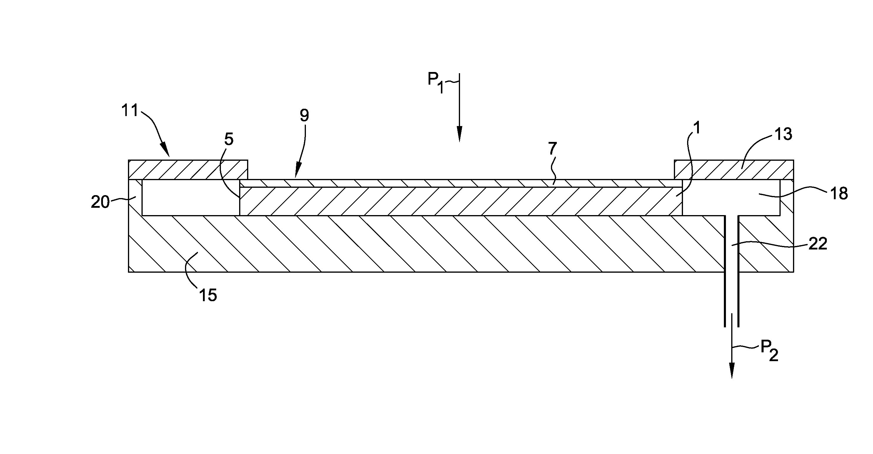
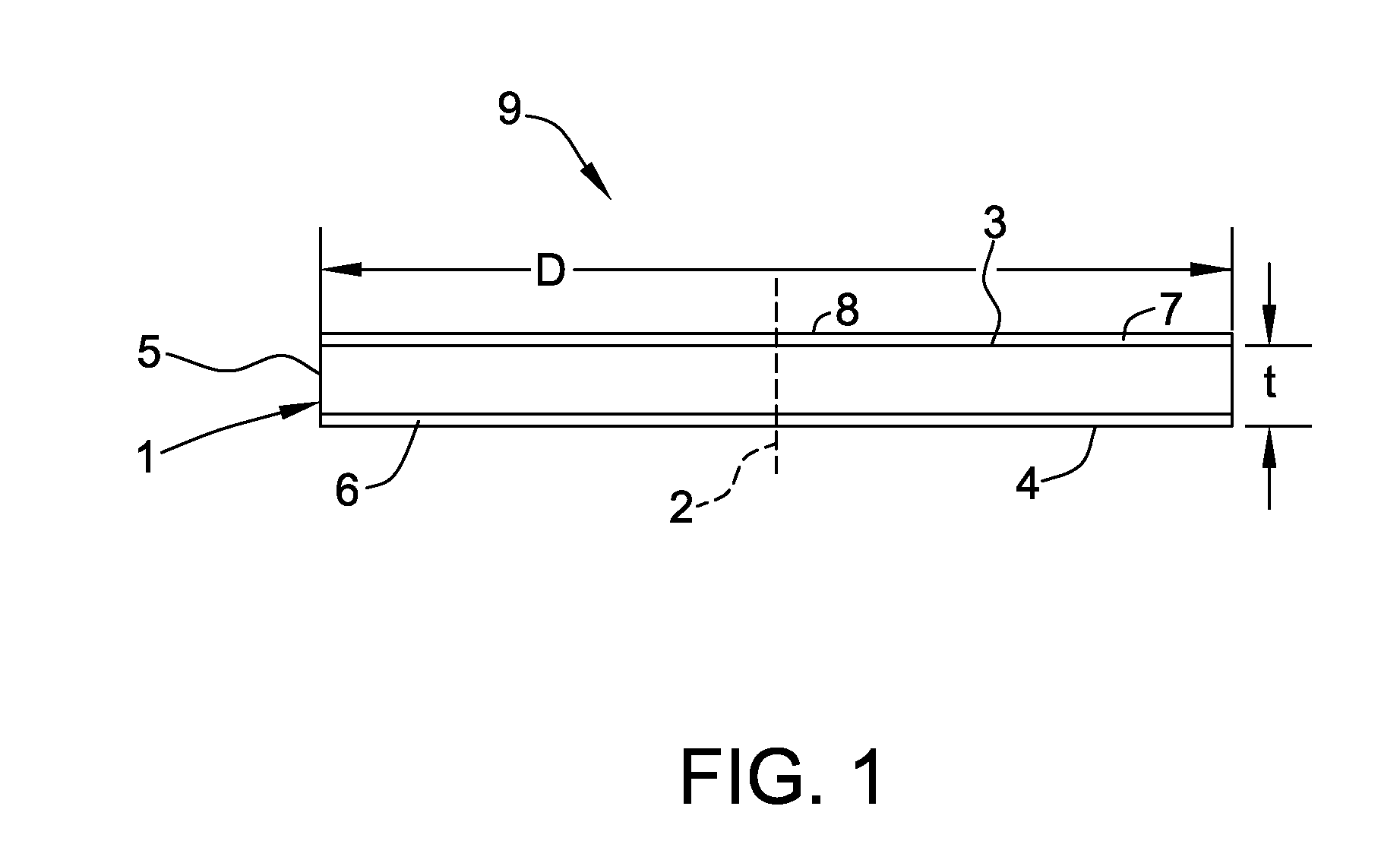
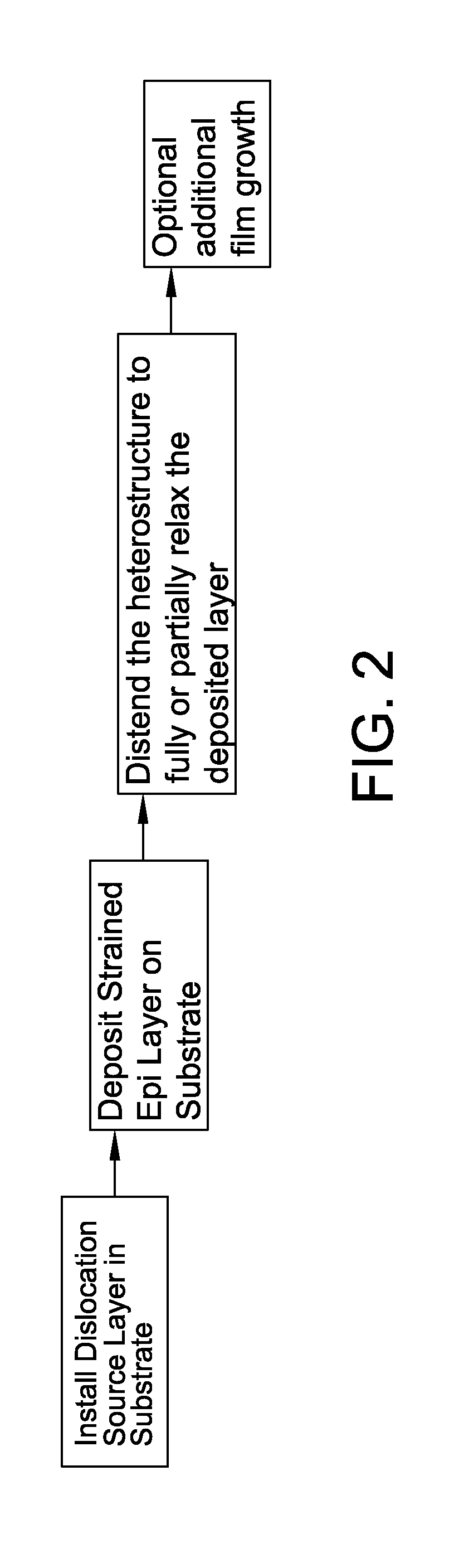
[0029]In accordance with one or more aspects of the present disclosure, heterostructures with reduced strain between the substrate and a surface layer having a different lattice constant than the substrate may be prepared such as by the process of FIG. 2. The surface layer may also be referred to herein as an “epitaxial layer”, “heteroepitaxial layer”, “deposited film”, “film”, “heterolayer” or “deposited layer”. A heterostructure having a substantially relaxed surface layer and a reduced concentration of misfit dislocations, also referred to as threading dislocations, may be formed.

[0030]In general, the processes of the present disclosure may include forming a dislocation source layer in a semiconductor substrate, depositing a heterolayer on the substrate before or after formation of the dislocation source layer and radially distending the heterostructure to generate (i.e., “activate”) dislocations and glide the dislocations from the dislocation source layer toward the surface laye...


PUM

PropertyMeasurementUnit
diameteraaaaaaaaaa
diameteraaaaaaaaaa
diameteraaaaaaaaaa

Abstract

Apparatus and processes for preparing heterostructures with reduced strain are disclosed. The heterostructures may include a semiconductor structure that conforms to a surface layer having a different crystal lattice constant than the structure to form a relatively low-defect heterostructure.

Description

CROSS-REFERENCE TO RELATED APPLICATIONS[0001]The present application claims the benefit of U.S. Provisional Application No. 61 / 747,613, filed Dec. 31, 2012; of U.S. Provisional Application No. 61 / 793,999, filed Mar. 15, 2013; of U.S. Provisional Application No. 61 / 790,445, filed Mar. 15, 2013 and of U.S. Provisional Application No. 61 / 788,744 filed Mar. 15, 2013, each of which is incorporated herein by reference.FIELD OF THE DISCLOSURE[0002]The present disclosure relates generally to preparation of semiconductor heterostructures with reduced strain and, in particular, to heterostructures with a semiconductor substrate that conforms to a surface layer having a different crystal lattice constant than the substrate, thereby forming a relatively low-defect heterostructure.BACKGROUND[0003]Multi-layered structures comprising a device layer with a device quality surface and a substrate that has a different crystal lattice structure than the material of the device layer are useful for a num...

Claims


Application Information

Patent Timeline
Patent Type & Authority Applications(United States)
IPC IPC(8): H01L21/322H01L21/302
CPCH01L21/302H01L21/322C30B25/12H01L21/68735H01L21/6875H01L21/67092H01L21/6838
Inventor FALSTER, ROBERT J.VORONKOV, VLADIMIR V.PITNEY, JOHN A.ALBRECHT, PETER D.
Owner GLOBALWAFERS CO LTD
Why Eureka
Try Eureka