

Semiconductor device including misfet
a semiconductor field effect transistor and semiconductor technology, applied in the field of semiconductor devices, can solve problems such as increased junction leakage current or contact failure, uneven contact resistance, and increased junction leakage curren
- Summary
- Abstract
- Description
- Claims
- Application Information
AI Technical Summary
Problems solved by technology
Method used
Image

Examples
embodiment 1
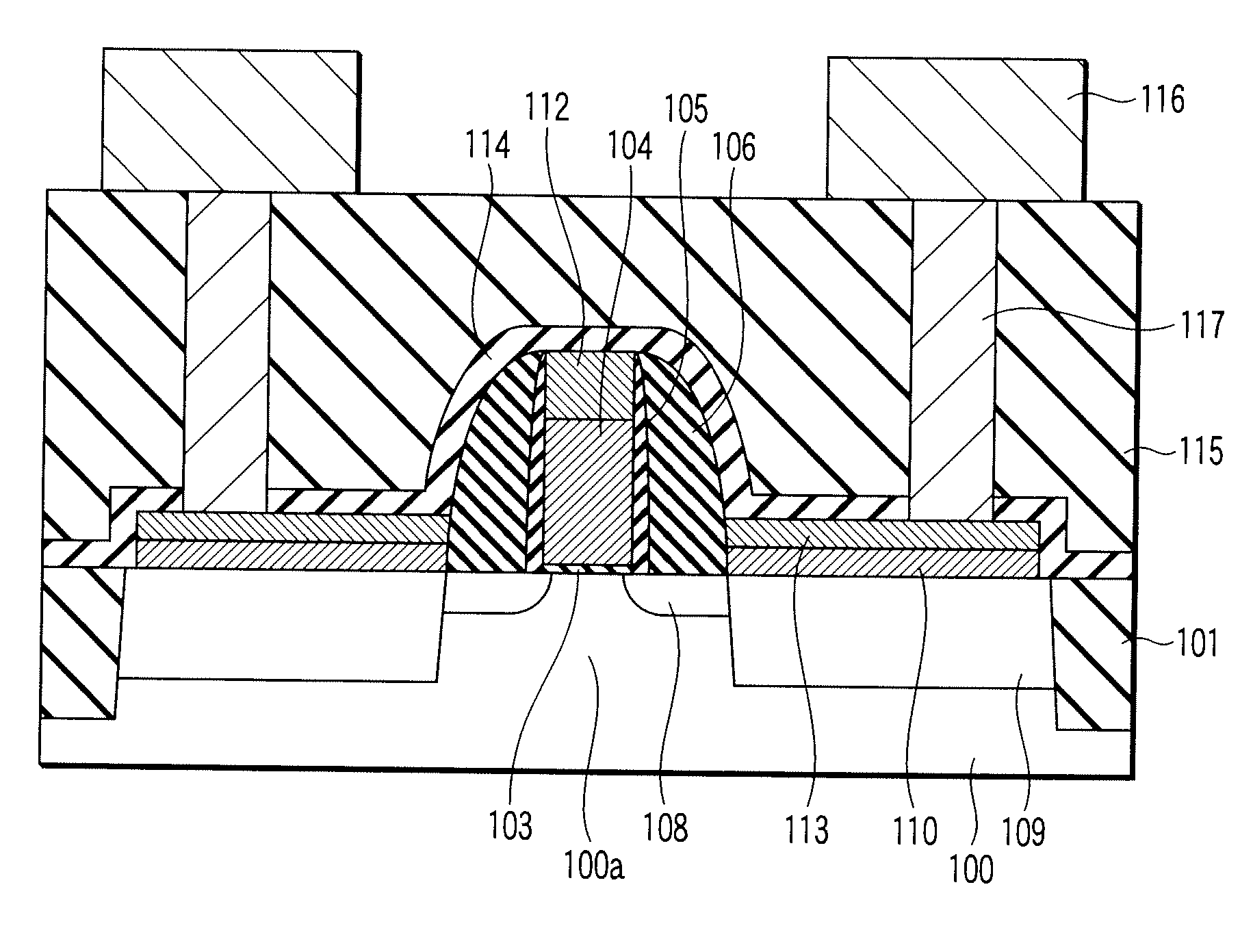
[0020] First, referring to FIG. 1, a structure of a semiconductor device according to Embodiment 1 of the present invention will be explained. FIG. 1 is a cross-sectional view showing a semiconductor device according to this embodiment that functions as a pMOS of a CMOSFET.
[0021] As shown in FIG. 1, an element isolating region 101 is provided in a semiconductor substrate, e.g., a single-crystal silicon semiconductor substrate (which will be referred to as a silicon substrate hereinafter) 100, and an element forming region 100a is partitioned by this element isolating region 101. A gate electrode 104 is formed on the silicon substrate 100 via a gate insulating film 103. A first sidewall insulating film 105 is formed on a side surface of the gate electrode 104, and a second sidewall insulating film 106 is formed on a side surface of the first sidewall insulating film 105.
[0022] Further, a first source / drain layer 108 as an extension layer in which a p-type impurity ion is implanted ...
embodiment 2
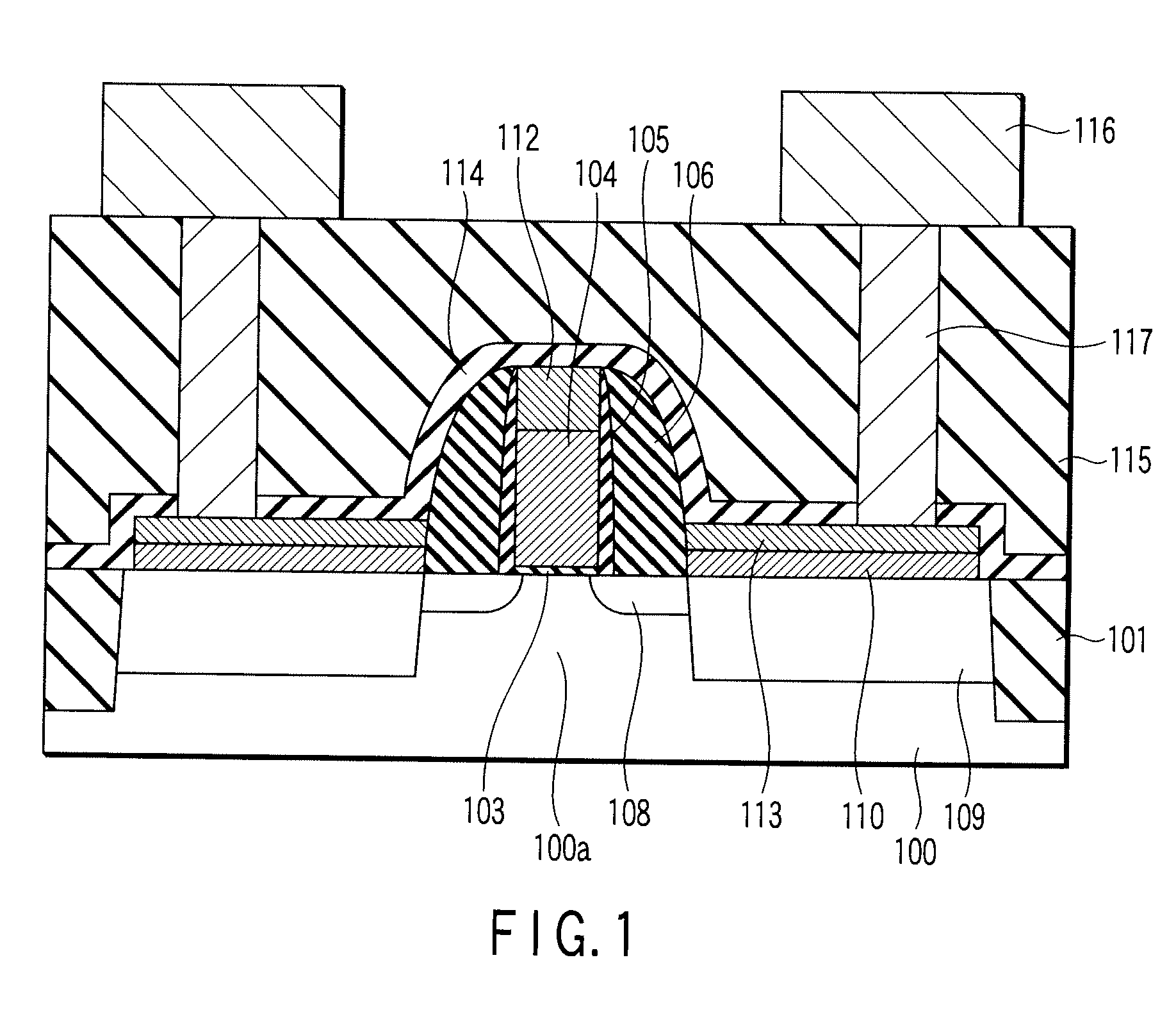
[0046] A structure of a semiconductor device according to Embodiment 2 of the present invention will be first explained with reference to FIG. 10. FIG. 10 is a cross-sectional view showing a semiconductor device according to this embodiment that functions as a pMOS of a CMOSFET.
[0047] As shown in FIG. 10, an element isolating region 101 is provided in a single-crystal silicon semiconductor substrate (a silicon substrate) 100, and an n-type well region 102 having an n-type impurity ion is formed in an element forming region 100 partitioned by this element isolating region 101. A gate insulating film 103 is formed on the n-type well region 102 of the silicon substrate 100, and a gate electrode 104 is formed on the gate insulating film 103. A first sidewall insulating film 105 is formed on a side surface of the gate electrode 104, and a second sidewall insulating film 106 is formed on a side surface of the first sidewall insulating film 105.
[0048] Additionally, a semiconductor layer ...
modification 1
of Embodiment 2
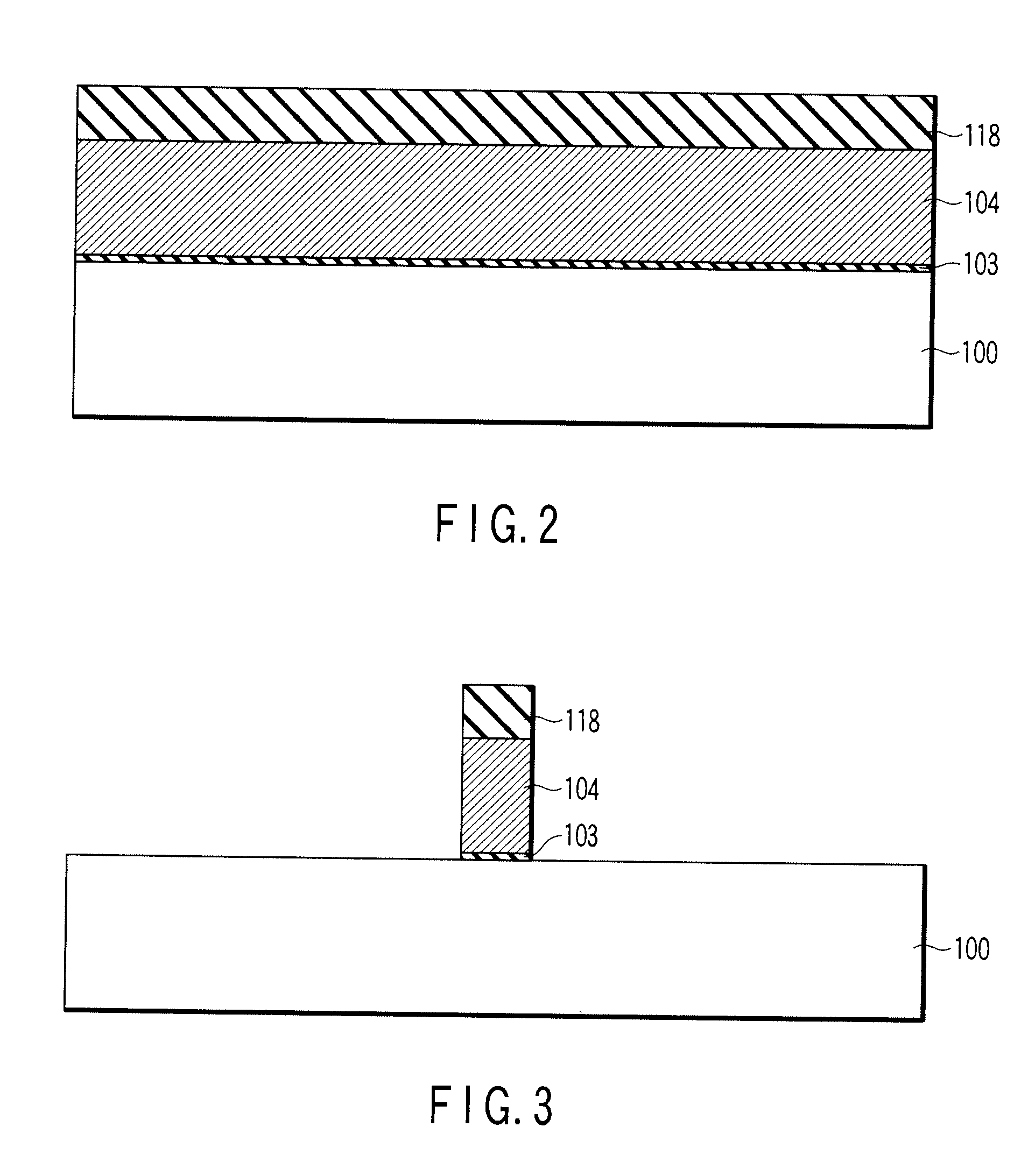
[0072]FIG. 14 is a cross-sectional view of a semiconductor device according to Modification of Embodiment 2.
[0073] The semiconductor device according to this modification is different from the semiconductor device according to Embodiment 2 in that a thickness of a first source / drain layer 108 as an extension layer is substantially the same as a thickness of a semiconductor layer 107 below a second sidewall insulating film 106. Therefore, in the following description of the semiconductor device according to this modification, like reference numerals denote parts equal to those in the structure and the manufacturing method of the semiconductor device according to Embodiment 2, thereby omitting a detailed explanation thereof.
[0074] That is, a first source / drain layer 108 in a semiconductor device according to this modification is formed by doping, e.g., boron (B) simultaneously with selective epitaxial grow of a silicon germanium layer as a semiconductor layer 107. The...
PUM
 Abstract
Description
Claims
Application Information