Display backplane having multiple types of thin-film-transistors

Active Publication Date: 2015-08-27
LG DISPLAY CO LTD
View PDF3 Cites 6 Cited by
  • Summary
  • Abstract
  • Description
  • Claims
  • Application Information

AI Technical Summary

Benefits of technology

[0012]In view of the problems above, inventors of the embodiments in the present disclosure recognized that there is a limit in providing displays with a higher resolution at a lower power consumption with conventional TFT backplane employing a

Problems solved by technology

However, a-Si TFT has low carrier mobility, and thus making a high speed backplane for a display is difficult with a-Si TFTs.
Due to the polycrystalline nature of its active layer, however, LTPS TFTs tend to have larger variations in threshold voltage (Vth) among the TFTs in a backplane, which can lead to display non-uniformity referr

Method used


Image

  • Display backplane having multiple types of thin-film-transistors
  • Display backplane having multiple types of thin-film-transistors
  • Display backplane having multiple types of thin-film-transistors

Examples


Embodiment Construction

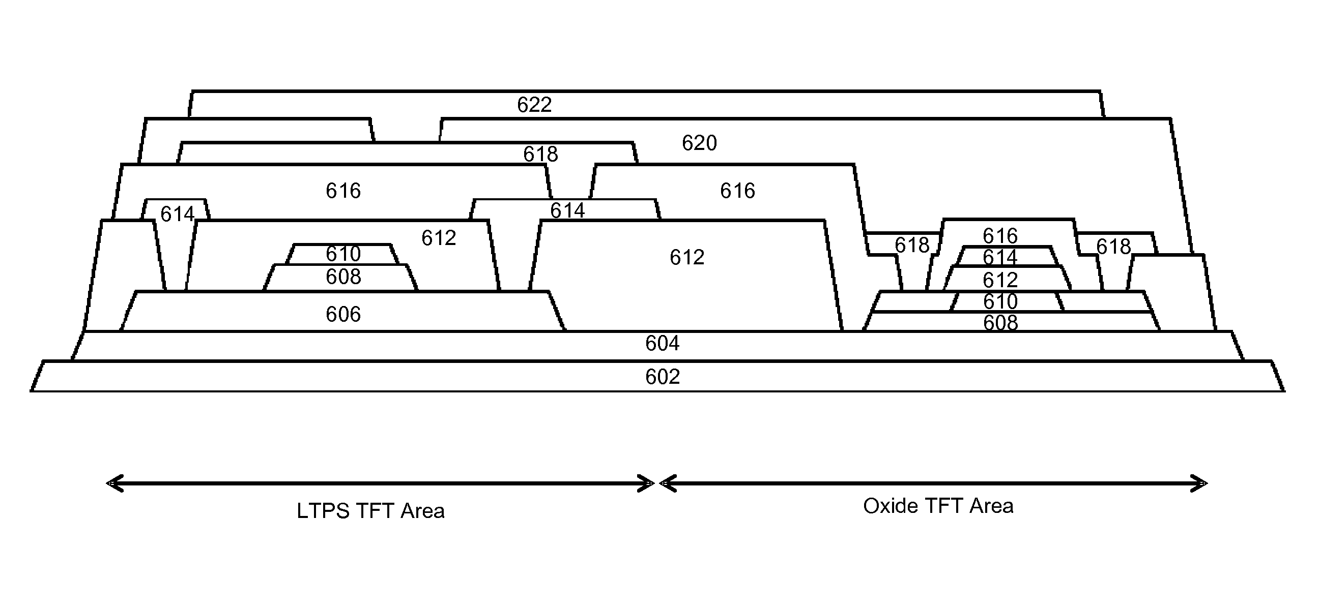
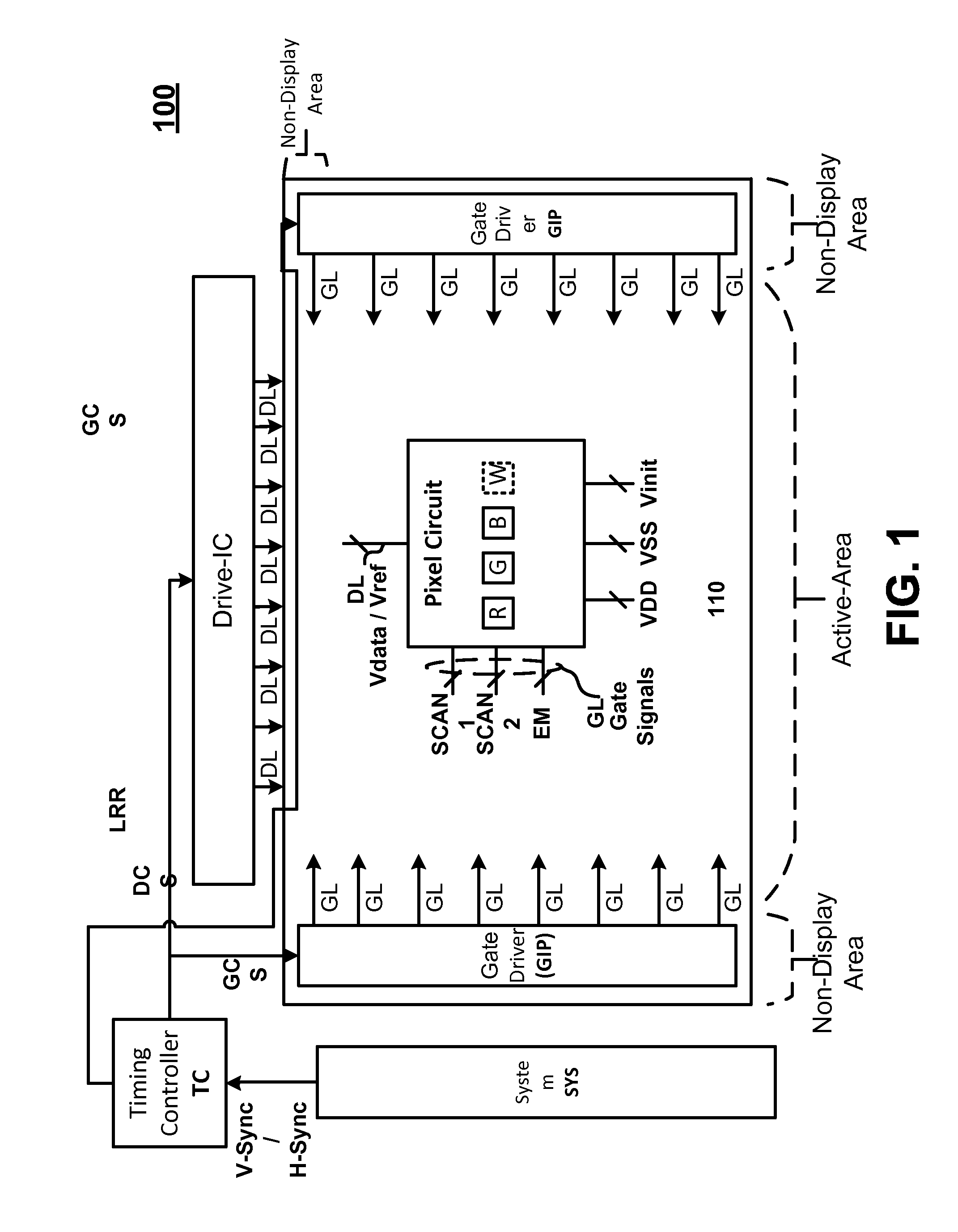
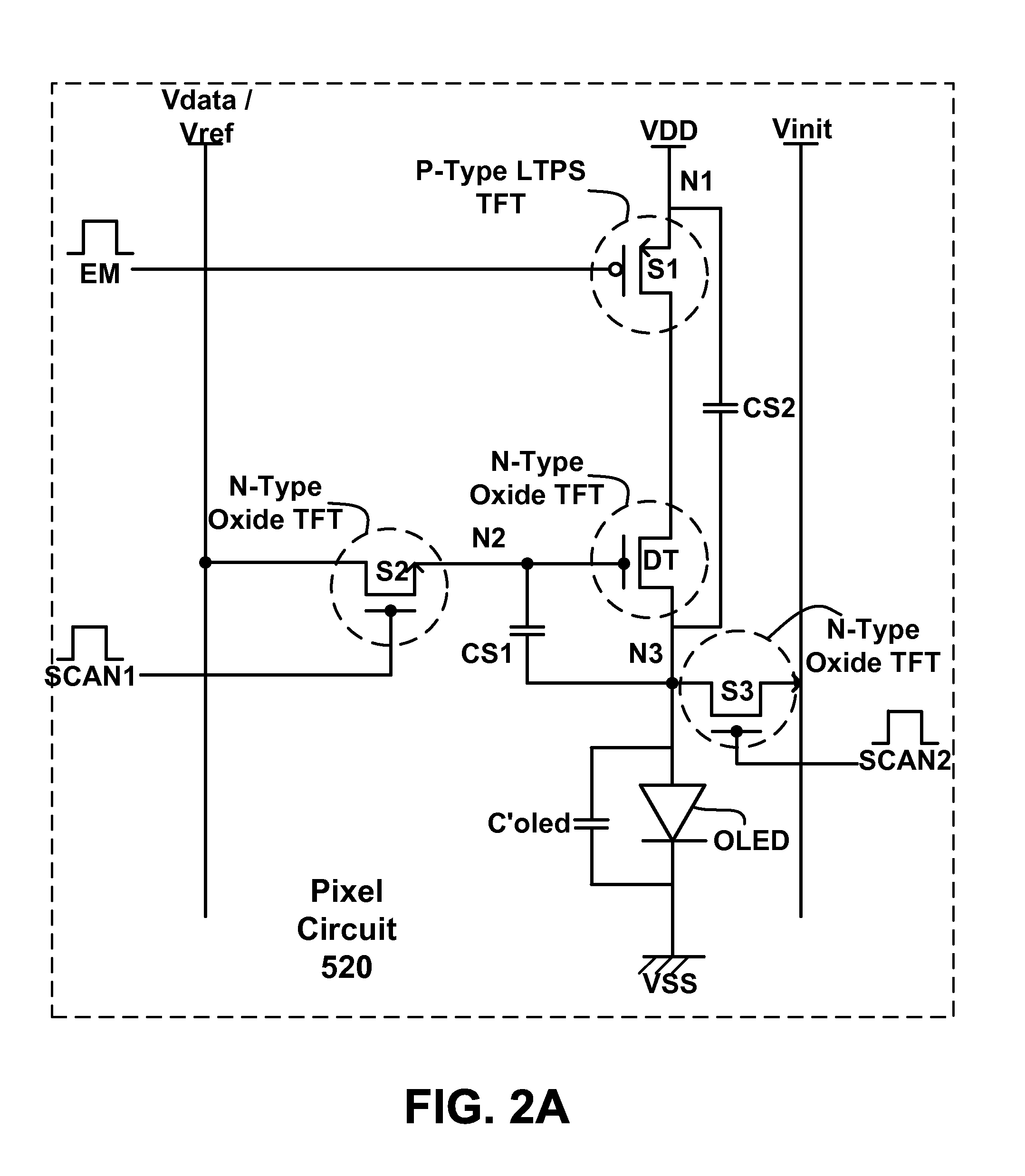
[0029]Various features and advantages described in the present disclosure will be more clearly understood from the following description with reference to the accompanying drawings. Note that the accompanying drawings are merely illustrative and may not be drawn to scale for easier explanation. Also, components having the same or similar function may be denoted by the same reference symbols / numeral throughout the drawings for describing various embodiments. The descriptions of the same or similar components may be omitted.

[0030]It will be understood that when an element as a layer, region or substrate is referred to as being “on” or “over” another element, it can be directly on the other element or intervening elements may also be present. In contrast, when an element is referred to as being “directly on” or “directly over” another element, there are no intervening elements present. It will also be understood that when an element is referred to as being “connected” or “coupled” to a...


PUM


Abstract

There is provided a TFT backplane having at least one TFT with oxide active layer and at least one TFT with poly-silicon active layer. In the embodiments of the present disclosure, at least one of the TFTs implementing the circuit of pixels in the active area is an oxide TFT (i.e., TFT with oxide semiconductor) while at least one of the TFTs implementing the driving circuit next to the active area is a LTPS TFT (i.e., TFT with poly-Si semiconductor).

Description


Claims


Application Information

Patent Timeline
Owner LG DISPLAY CO LTD
Why Eureka
Try Eureka