
Marking apparatus and marking method for display panel

a marking apparatus and display panel technology, applied in the field of display technology, can solve the problems of inconvenient marking, inability to specifically correct the marking to a pixel, and inability to generate numerous defective display panels, and achieve the effect of accurately locating and sampling, and accurate marking

Inactive Publication Date: 2015-09-17
BOE TECH GRP CO LTD +1
View PDF6 Cites 8 Cited by
  • Summary
  • Abstract
  • Description
  • Claims
  • Application Information

AI Technical Summary

Benefits of technology

The present invention provides a marking apparatus and a marking method for a display panel that can accurately mark the position where a defect occurs. This allows for convenient analysis and positioning of the defect for repair or replacement. The technical effect is improved accuracy in identifying and identifying the root cause of display panel defects.

Problems solved by technology

In the production process of thin film transistor-liquid crystal displays (TFT-LCDs), it is inevitable to generate numerous defective display panels (for example, with moiré or abnormal pixel points).
However, in the process of manually marking the positions where the defects occur on the display panels to be marked with marker pens, it is found that the accuracy of marking cannot be specifically corrected to a pixel due to too large range of manual marking, and meanwhile, marking is made inconveniently because approximate locations where the defects occur need to be determined with naked eyes through microscopic lens during marking.

Method used


Image

  • Marking apparatus and marking method for display panel
  • Marking apparatus and marking method for display panel
  • Marking apparatus and marking method for display panel

Examples


embodiment 1

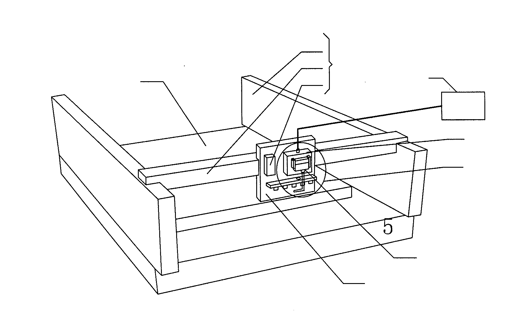
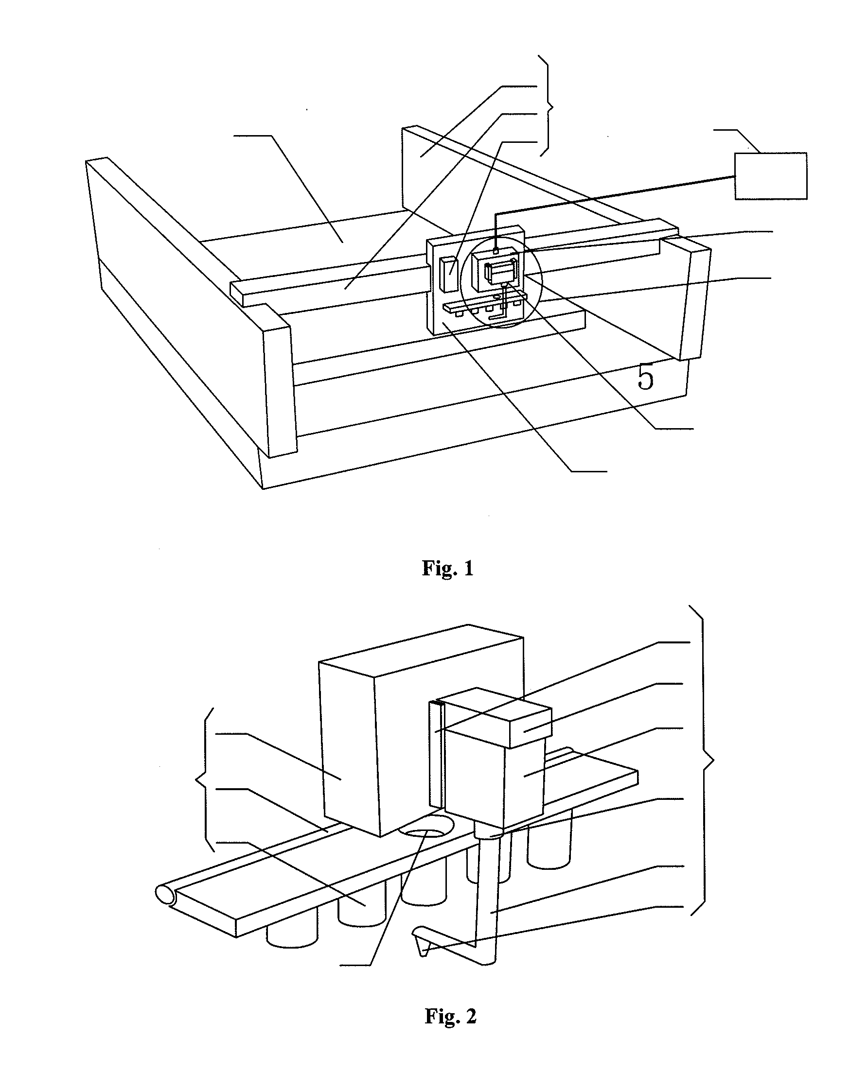
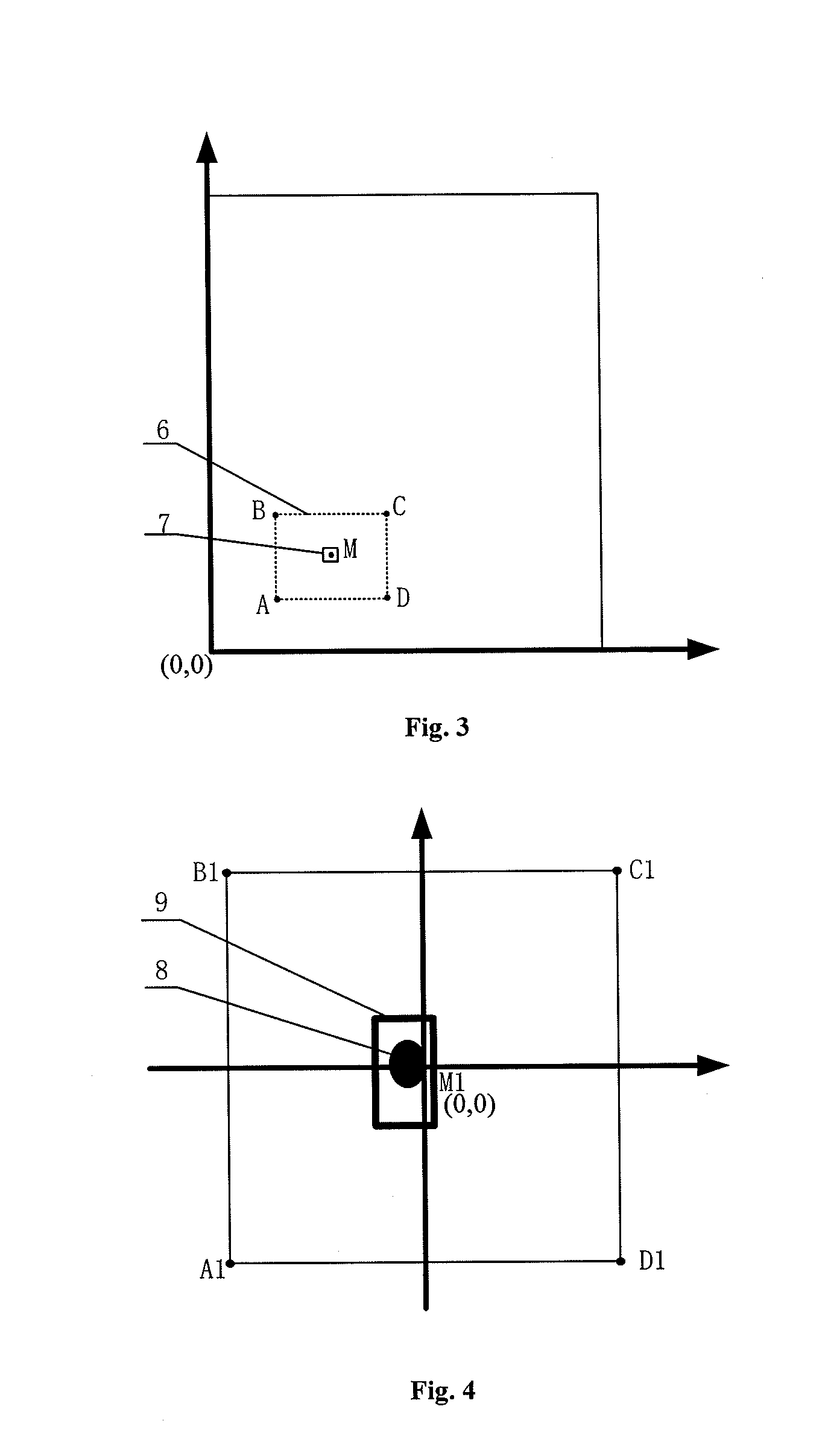
[0034]FIG. 1 is a diagram illustrating a structure of a marking apparatus for a display panel provided by Embodiment 1 of the present invention. FIG. 2 is an enlarged view of a structure Q in FIG. 1. FIG. 3 is a schematic diagram of a coordination system for a region containing a position where a defect occurs on a display panel to be marked. FIG. 4 is a schematic diagram of a coordinate system for the simulated image. As shown in FIGS. 1 to 4, the marking apparatus comprises a driving module 1, an image acquiring module 2, a simulated marking module 3 and a real marking module 4. The driving module 1 is connected to the image acquiring module 2, the image acquiring module 2 is connected to the simulated marking module 3, and the simulated marking module 3 is connected to the real marking module 4. The driving module 1 is configured to drive the image acquiring module 2 so as to move it to be above a position 8 where a defect occurs on the display panel 5 to be marked. The image acq...


PUM


Abstract

The present invention provides a marking apparatus for a display panel and a marking method for a display panel. The marking device comprises an image acquiring module, a simulated marking module and a real marking module. A simulated marking line is drawn, by the simulated marking module, in an image acquired by the image acquiring module, of a region containing a position where a defect occurs on a display panel to be marked. The real marking module automatically draws a real marking line on the display panel to be marked according to the simulated marking line. Thus, a position where a defect occurs on a display panel to be marked is accurately marked, and it is convenient for an engineer to accurately locate and sample the defective position in the subsequent analysis process.

Description

FIELD OF THE INVENTION[0001]The present invention relates to the field of display technology, and particularly relates to a marking apparatus for a display panel and a marking method for a display panel.BACKGROUND OF THE INVENTION[0002]In the production process of thin film transistor-liquid crystal displays (TFT-LCDs), it is inevitable to generate numerous defective display panels (for example, with moiré or abnormal pixel points). To reduce defective rate, improve yield rate and reduce loss, engineers need to analyze positions where defects occur on display panels, and usually need to sample and analyze defects. During sampling, engineers need to determine positions where the defects occur at first and then mark the positions.[0003]Specifically, an engineer observes a display panel through a microscope, find a position where a defect occurs on the display panel and then manually marks the position with a marker pen.[0004]However, in the process of manually marking the positions wh...

Claims


Application Information

Patent Timeline
Patent Type & Authority Applications(United States)
IPC IPC(8): G06T7/00H04N5/225G02B13/00
CPCG06T7/0004H04N5/2254G02B13/0015G01N21/8851G01N2021/8861G01N2021/888
Inventor LIN, ZIJINDENG, CHAOYANGTIAN, CHAO
Owner BOE TECH GRP CO LTD
Learn More