Chip card inlay for contact-activated and contactlessly activated chip cards

a technology of contact activation and chip card, which is applied in the field of contact activation and contactless activation chip card inlay, can solve the problems of textile fabric ups, downs, uneven surface of textile fabric, etc., and achieve the effect of improving the chip connection

Active Publication Date: 2015-09-24
SES RFID SOLUTIONS
View PDF0 Cites 0 Cited by
  • Summary
  • Abstract
  • Description
  • Claims
  • Application Information

AI Technical Summary

Benefits of technology

[0006]It is therefore the object of the invention to create a chip card inlay which improves the connection of the chip at the antenna ends.
[0009]Via a conductive paste or a conductive film, which is applied to the textile fabric and follows the unevennesses of the surface, a three-dimensionally conductive terminal pad structure is formed. Alternatively, threads of the textile fabric may be conductive, for example on account of the use of stainless steel, silver, etc., as a result of which a three-dimensionally conductive terminal pad structure can already be formed over the textile fabric itself. A surface contour of the respective conductive pad with the weave points of the textile fabric as topographical contact zone elevations on the conductive contact zone results in a considerable improvement in the attachment of the chip to the conductive pad. The adhesion to an adhesive which connects the chip or the chip lugs thereof to the conductive pads is considerably enhanced according to the invention.
[0010]As a result, the use of a hotmelt adhesive is possible, with the result that the production of the chip cards is easier and quicker. The mechanical interlock which the cooled adhesive creates at the adhesive / conductive pad interface, produces a permanent and stable adhesive bond.

Problems solved by technology

The textile fabric thus has ups, downs and irregularities, caused by the threads, which bring about an uneven surface of the textile fabric.

Method used


Image

  • Chip card inlay for contact-activated and contactlessly activated chip cards
  • Chip card inlay for contact-activated and contactlessly activated chip cards

Examples


Embodiment Construction

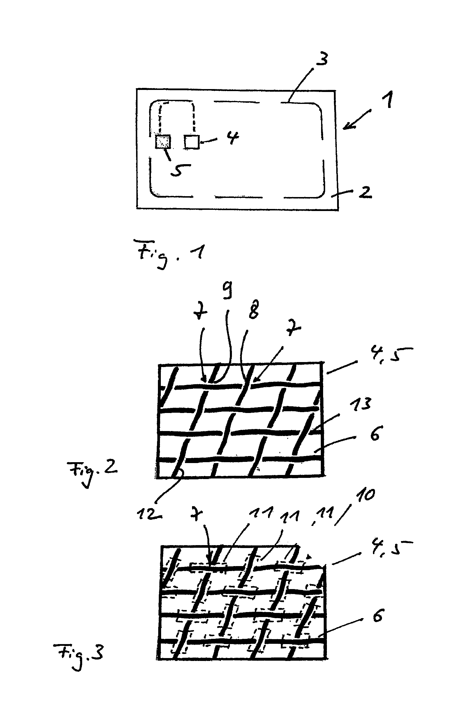
[0017]FIG. 1 shows a chip card inlay 1 for contact-activated and contactlessly activated chip cards, having a planar substrate layer 2 made of a non-conductive plastics material. Fastened to the substrate layer 2 is an antenna 3 having, at its end, planar conductive pads 4, 5 for attaching a chip (not illustrated). The antenna 3 is, in a known manner, preferably a planar coil.

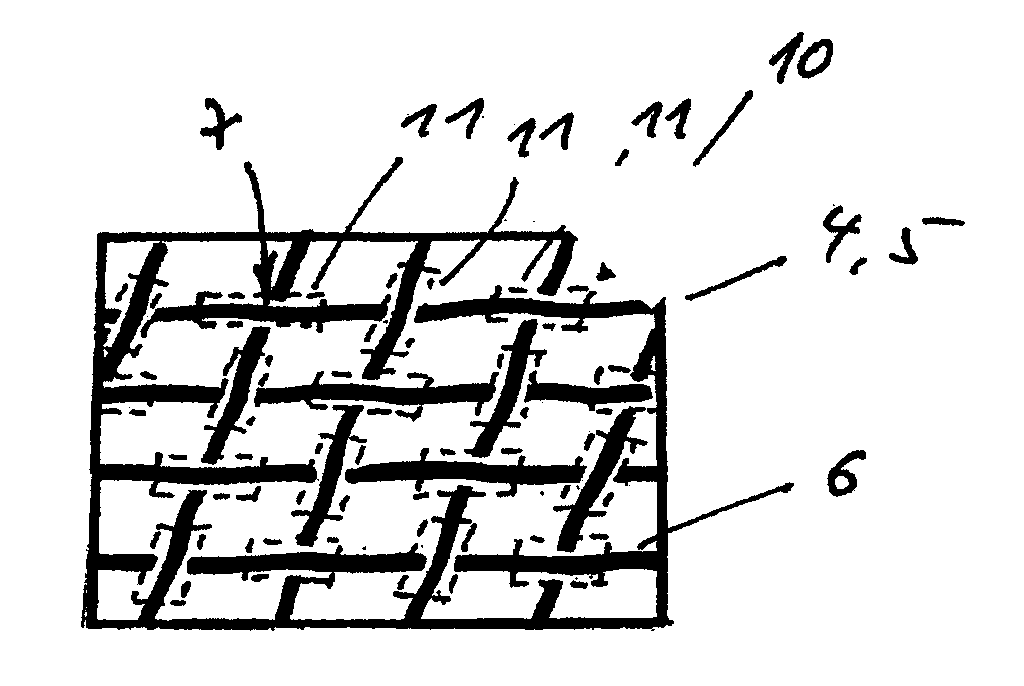
[0018]As FIG. 2 shows, the conductive pads 4, 5 are formed from a textile fabric 6 having thread crossings 7, the weave points of which may be in the form of a raised thread 8 or lowered thread 9. As FIG. 3 shows, an electrically conductive contact zone 10 is provided on the respective face of the textile fabric 6, said electrically conductive contact zone 10 having a three-dimensionally conductive terminal pad structure with the weave points of the textile fabric as topographical contact zone elevations 11, for attaching a chip.

[0019]In order to form the conductive contact zone 10, the textile fabric 6 of the ...


PUM


Abstract

Chip card inlay for contact-activated and contactlessly activated chip cards, having a planar substrate layer made of a non-conductive plastics material, on which an antenna having, at its end, planar conductive pads for attaching a chip is fastened, wherein the conductive pads are formed from a textile fabric having thread crossings, and on each top side of the textile fabric an electrically conductive contact zone is provided which has a three-dimensionally conductive terminal pad structure with weave points of the textile fabric as topographical contact zone elevations.

Description

CROSS-REFERENCES TO RELATED APPLICATIONS[0001]This application is a continuation of U.S. patent application Ser. No. 14 / 179,091, filed Feb. 12, 2014, which claims priority to European Application No. EP 13 001 267.71, filed Mar. 13, 2013, the complete disclosures of which are herein incorporated by reference.BACKGROUND OF THE INVENTION[0002]The invention relates to a chip card inlay for contact-activated and contactlessly activated chip cards.[0003]Chip cards are special plastic cards having a chip which contains hardware logic, a memory or a microprocessor. Such chip cards are controlled by special card readers. Such contact chip cards are susceptible to faults on account of wear or soiling and react in a sensitive manner to vibrations which can result in brief contact interruptions. Therefore, in addition to contact chip cards, contactlessly activated chip cards, known as transponder cards, are also known, which combine two technologies for automatic identification and data acquis...

Claims


Application Information

Patent Timeline
Patent Type & Authority Applications(United States)
IPC IPC(8): G06K19/077
CPCG06K19/0723G06K19/07769G06K19/07754
Inventor SCATTERGOOD, MARTIN
Owner SES RFID SOLUTIONS
Why Eureka
Try Eureka