OpportunistIC placement of IC test strucutres and/or e-beam target pads in areas otherwise used for filler cells, tap cells, decap cells, scribe lines, and/or dummy fill, as well as product IC chips containing same

a technology of e-beam target pads and scribe lines, which is applied in the direction of individual semiconductor device testing, semiconductor/solid-state device testing/measurement, instruments, etc., can solve the problems of limited area available in the scribe line of product wafers, inability to accommodate certain types of test structures, and still less than ideal, so as to improve the coverage of test structures

Inactive Publication Date: 2015-09-24
PDF SOLUTIONS INC
View PDF2 Cites 92 Cited by
  • Summary
  • Abstract
  • Description
  • Claims
  • Application Information

AI Technical Summary

Benefits of technology

[0007]The present invention discloses several techniques for improving test structure coverage on product ICs with little or no sacrifice of active die area.

Problems solved by technology

While these and other known techniques that locate test structures on product wafers produce useful results, they are still less than ideal.
Specifically, the area available in the scribe line of product wafers is strictly limited and can only accommodate certain types of test structures.
Additionally, both the in-the-scribe-line and under-the-probe-pad methods suffer from the fact that the test structures are located far away from the most important active circuitry regions, and are thus not likely to accurately represent the processing environment of the active circuitry.
Although the '083 patent can potentially mitigate this problem, it does so at the unacceptable cost of requiring large, dedicated test regions (see '083 patent, FIG. 5, regions 44-45) that consume otherwise precious active die area.

Method used


Image

  • OpportunistIC placement of IC test strucutres and/or e-beam target pads in areas otherwise used for filler cells, tap cells, decap cells, scribe lines, and/or dummy fill, as well as product IC chips containing same
  • OpportunistIC placement of IC test strucutres and/or e-beam target pads in areas otherwise used for filler cells, tap cells, decap cells, scribe lines, and/or dummy fill, as well as product IC chips containing same
  • OpportunistIC placement of IC test strucutres and/or e-beam target pads in areas otherwise used for filler cells, tap cells, decap cells, scribe lines, and/or dummy fill, as well as product IC chips containing same

Examples


Embodiment Construction

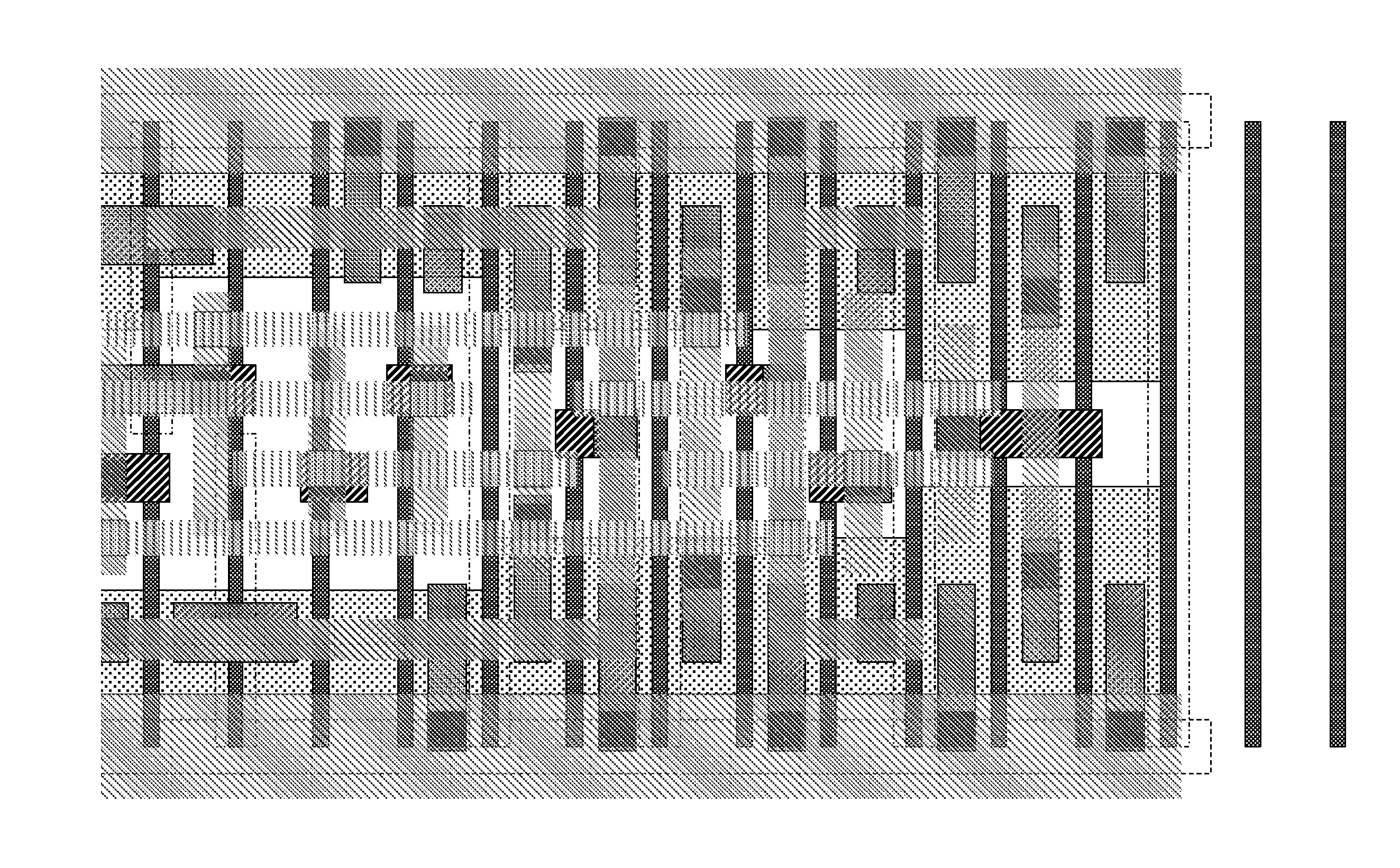
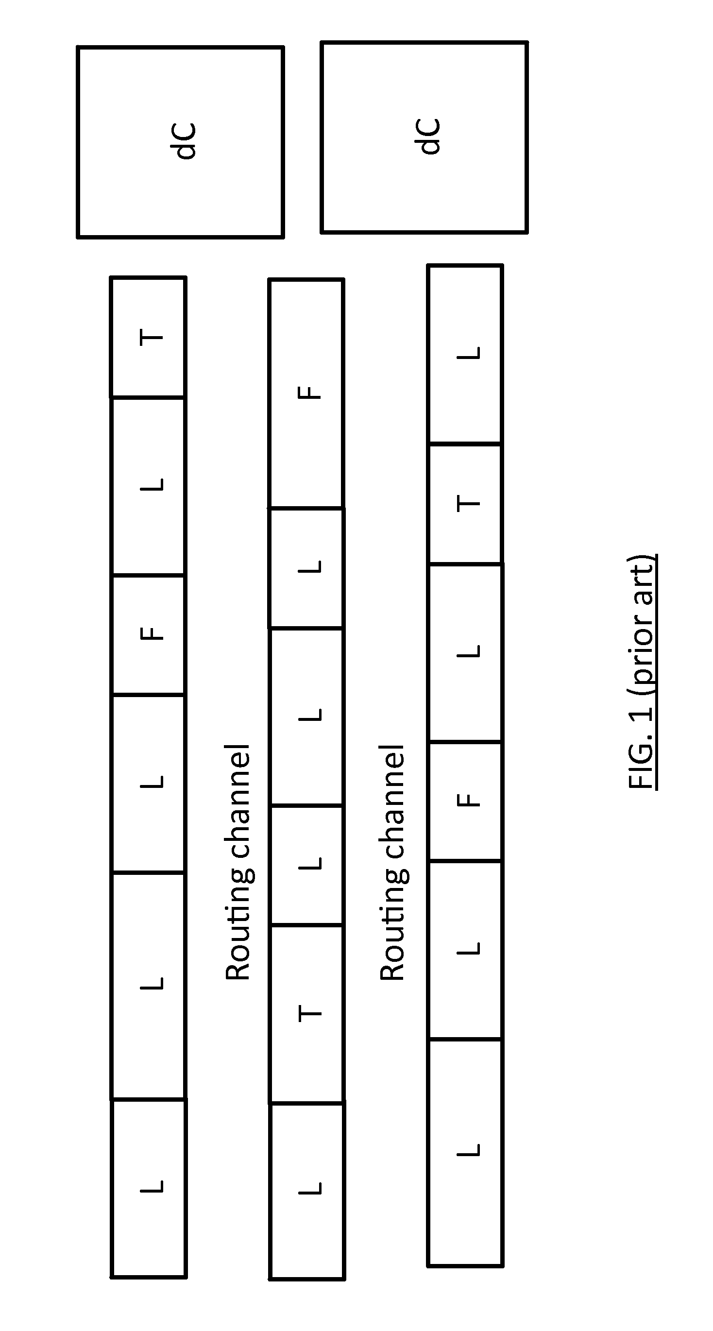
[0136]FIG. 1 conceptually depicts an illustrative section of a prior-art standard cell layout that includes logic cells (L), tap cells (T) and filler cells (F) arranged in rows, with routing channels between the rows, and nearby decap cells (dC). As depicted, the overall distribution of decap, tap and filler cells within this illustrative section is irregular and does not follow any obvious pattern or symmetry. (Persons skilled in the art will immediately recognize that the depictions herein are conceptual, and only intended to illustrate the principles of the invention, rather than represent actual layout realities. Indeed, such skilled artisans will appreciate that tap cells typically come in only one size and appear at regular or nearly regular intervals. Similarly, such skilled artisans will also recognize that decap cells can, and frequently are, sized to fit within and placed within the standard cell rows.)

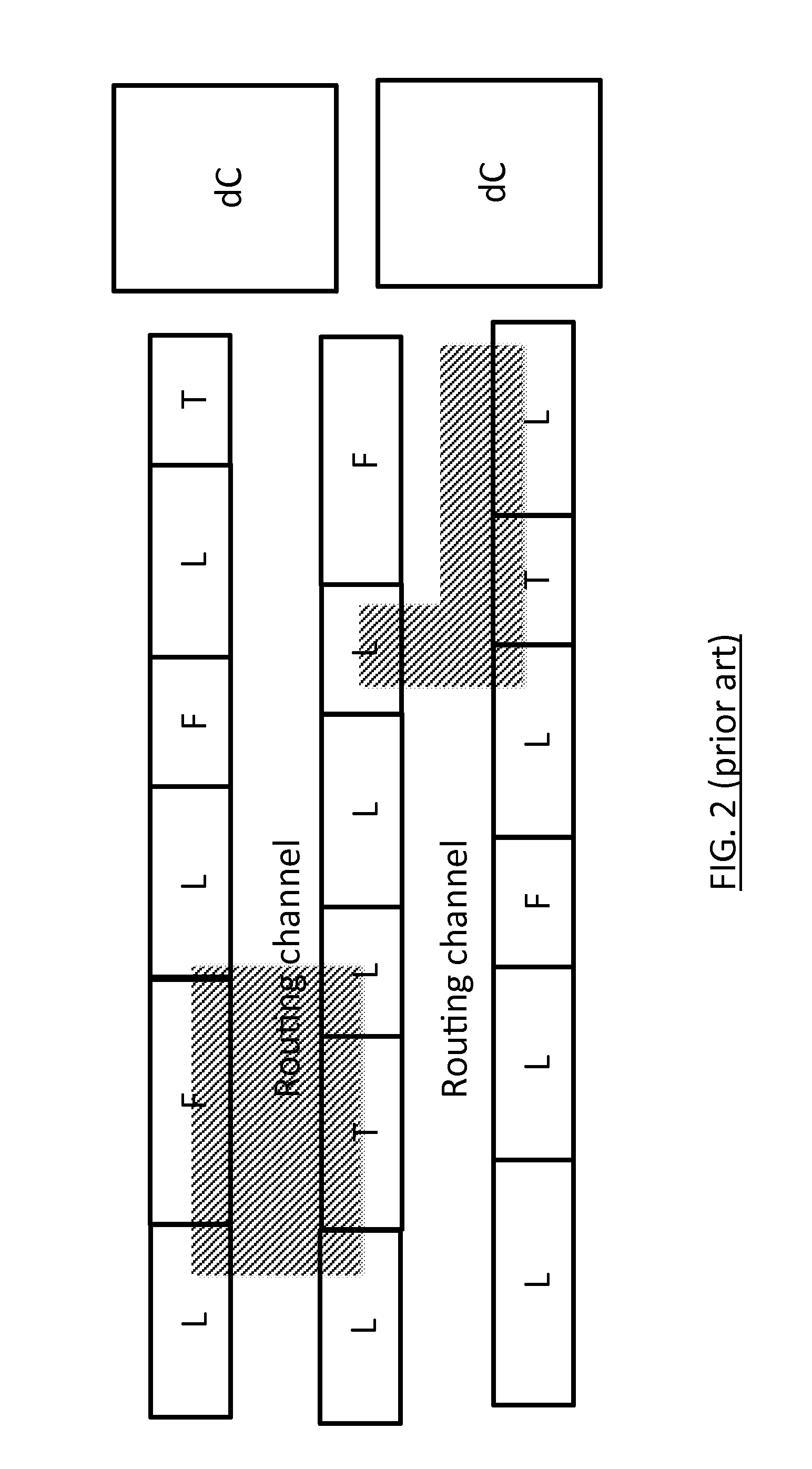
[0137]FIG. 2 conceptually depicts the same prior-art layout as FIG. 1, ...


PUM


Abstract

Product ICs/wafers include additional diagnostic, test, or monitoring structures opportunistically placed in filler cell positions, within tap cells, within decap cells, within scribe line areas, and/or within dummy fill regions. Improved fabrication processes utilize data from such structure(s) in wafer disposition decisions, rework decisions, process control, yield learning, or fault diagnosis.

Description

CROSS-REFERENCE TO RELATED APPLICATIONS[0001]This application is a continuation of U.S. patent application Ser. No. 14 / 303,578, filed Jun. 12, 2014, which '578 application is a continuation-in-part of U.S. patent application Ser. No. 14 / 190,040, filed Feb. 25, 2014, which is a continuation-in-part of U.S. patent application Ser. No. 14 / 038,799, filed Sep. 27, 2013. This application also claims priority from the following Provisional U.S. Patent Applications: Ser. No. 61 / 942,163, filed Feb. 20, 2014; Ser. No. 61 / 971,306, filed Mar. 27, 2014; Ser. No. 61 / 972,787, filed Mar. 31, 2014; Ser. No. 61 / 982,652, filed Apr. 22, 2014; and Ser. No. 62 / 011,161, filed Mar. 12, 2014. Each of the '578, '040, '799, '163, '306, '787, '652 and '161 applications is incorporated by reference herein.FIELD OF THE INVENTION[0002]This invention relates to the field of semiconductor integrated circuits and to methods for manufacturing and testing such circuits.BACKGROUND OF THE INVENTION[0003]Placement of “te...

Claims


Application Information

Patent Timeline
Patent Type & Authority Applications(United States)
IPC IPC(8): H01L21/66G01R31/26
CPCG01R31/26H01L22/10G01N23/2251H01L22/12H01L22/20H01L22/30G01R31/2644H01J37/147H01J37/20H01J37/222H01J37/285H01J2237/24592
Inventor DE, INDRANILCIPLICKAS, DENNIS J.LAM, STEPHENHAIGH, JONATHANROVNER, VYACHESLAV V.HESS, CHRISTOPHERBROZEK, TOMASZ W.STROJWAS, ANDRZEJ J.DOONG, KELVINKIBARIAN, JOHN K.LEE, SHERRY F.MICHAELS, KIMON W.STROJWAS, MARCIN A.O'SULLIVAN, CONORJAIN, MEHUL
Owner PDF SOLUTIONS INC
Why Eureka
Try Eureka