
Semiconductor package and manufacturing method thereof

Inactive Publication Date: 2015-10-01
CHIPMOS TECH INC
View PDF0 Cites 2 Cited by
  • Summary
  • Abstract
  • Description
  • Claims
  • Application Information

AI Technical Summary

Benefits of technology

The patent describes a method of making semiconductor packaging by using a carrier and a photosensitive material. The photosensitive material is put on the carrier and then exposed to create a layer with both conductive and insulating properties. A chip is then placed on top of this layer and connected to the conductive parts of it. The chip is then covered with an encapsulant and the carrier is removed. The technical effect of this method is to create a reliable and efficient way of packaging semiconductors.

Problems solved by technology

Therefore, the manufacturing process of the conventional printed circuit substrate is complex and time consuming, and the thickness of the printed circuit substrate can not be decreased effectively.

Method used


Image

  • Semiconductor package and manufacturing method thereof
  • Semiconductor package and manufacturing method thereof
  • Semiconductor package and manufacturing method thereof

Examples


Embodiment Construction

[0017]A detailed description of the hereinafter described embodiments of the disclosed apparatus and method are presented herein by way of exemplification and not limitation with reference to the Figures. Although certain embodiments are shown and described in detail, it should be understood that various changes and modifications may be made without departing from the scope of the appended claims. The scope of the present invention will in no way be limited to the number of constituting components, the materials thereof, the shapes thereof, the relative arrangement thereof, etc., and are disclosed simply as an example of embodiments of the present invention.

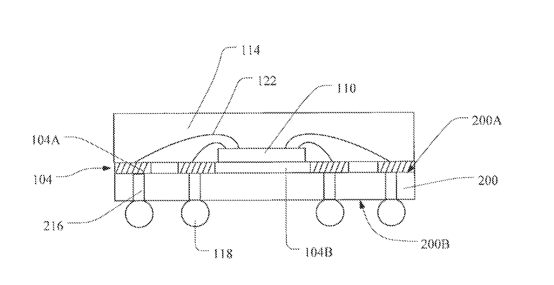
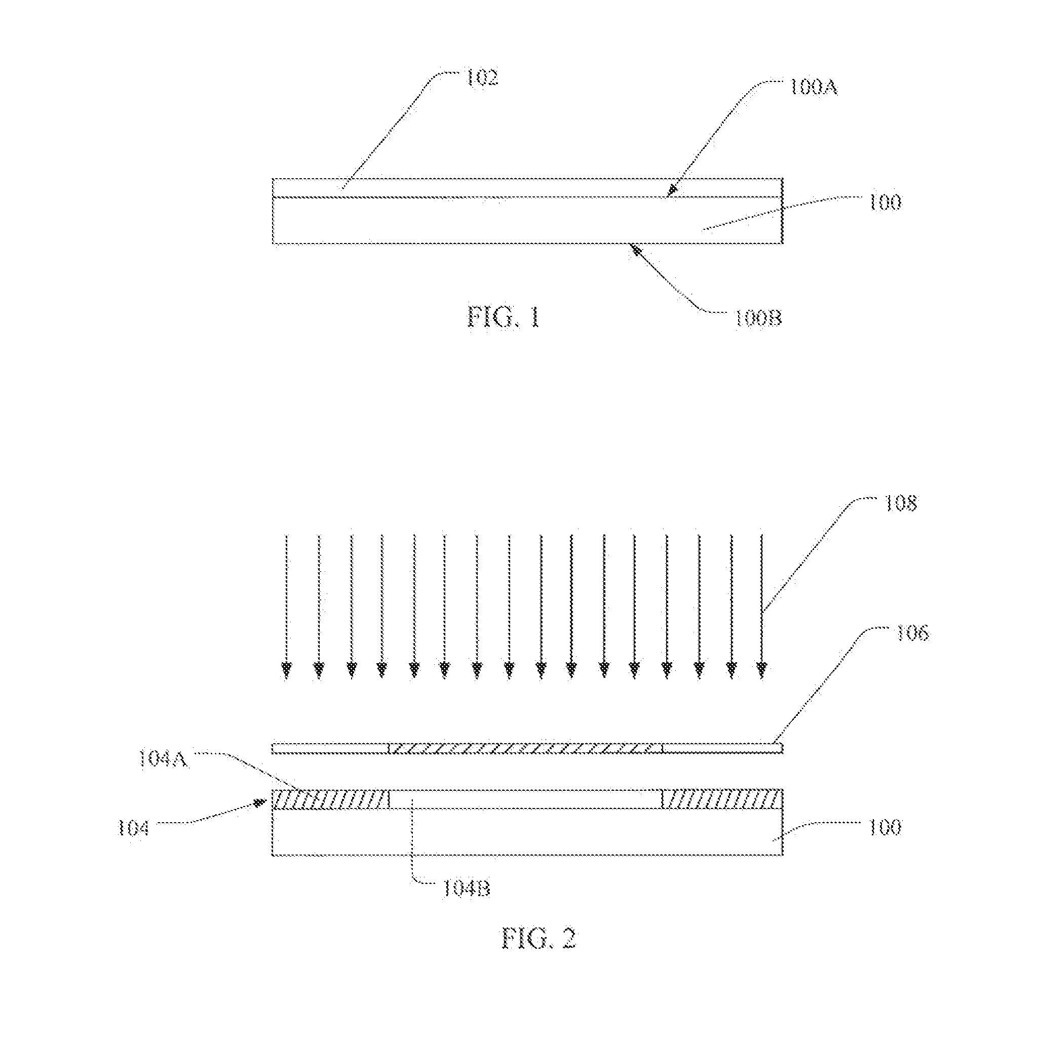
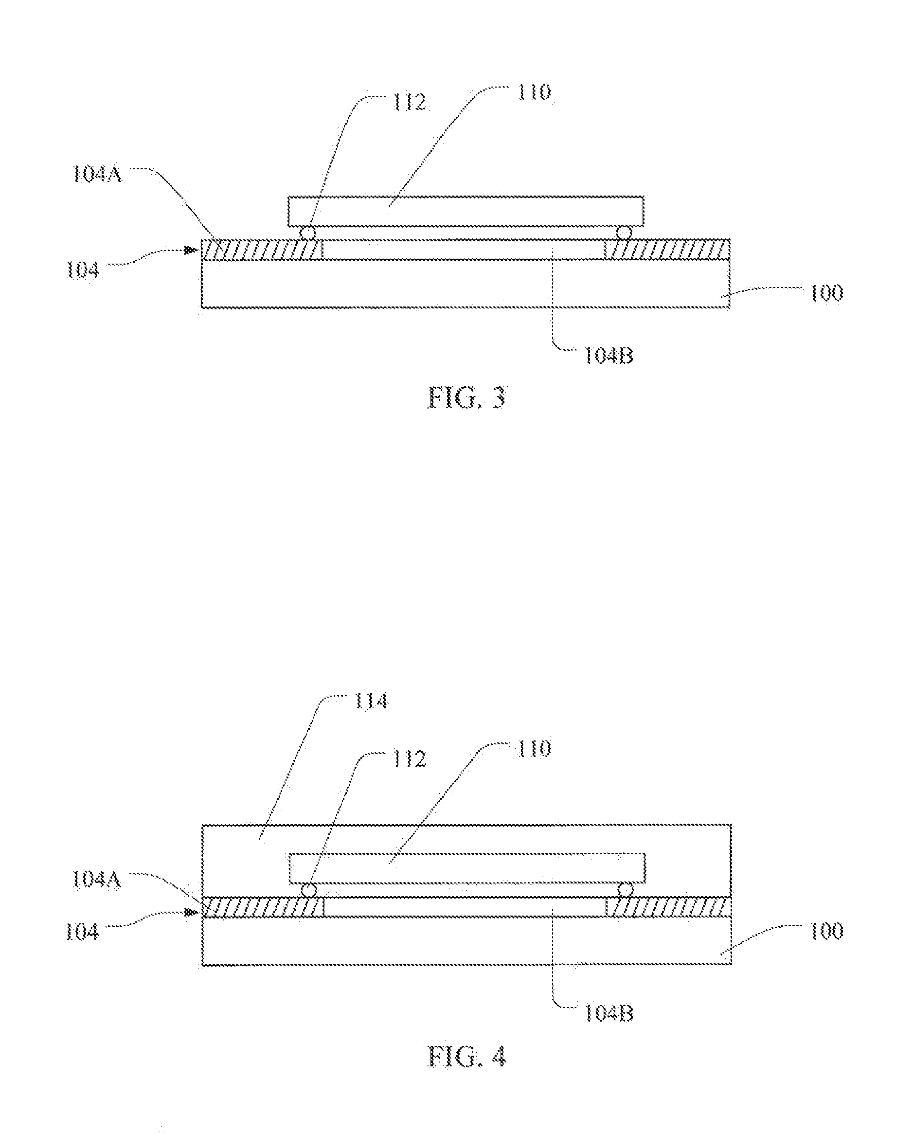
[0018]Please refer to FIG. 1 to FIG. 5, which show the sectional drawings of each step of a semiconductor packaging method, according to an embodiment of the present invention. Referring to FIG. 1, the packaging method of the present invention is performed on a carrier 100, wherein the carrier 100 has a first surface 100A and a s...


PUM


Abstract

A semiconductor package and manufacturing method thereof are disclosed. The semiconductor package includes a photosensitive conductive layer, a chip and an encapsulant. The photosensitive conductive layer includes at least one electrically conductive portion and at least one insulating portion. The chip is disposed on the photosensitive conduct layer and electrically coupled the least one electrically conductive portion. The encapsulant covers the chip and the photosensitive conductive layer.

Description

CROSS REFERENCE TO RELATED APPLICATION[0001]This application claims priority to Taiwan Patent Document No. 103111955, filed on Mar. 31, 2014 with the Taiwan Patent Office, which is incorporated by reference in its entirety.BACKGROUND OF THE INVENTION[0002]1. Field of the Invention[0003]The present invention relates to a semiconductor package and manufacturing method thereof, and more particularly, to a semiconductor package and manufacturing method thereof using a photosensitive conductive material as a circuit layer.[0004]2. Description of the Prior Art[0005]With the rapid development of technology, the semiconductor packaging technology and materials change rapidly as well. As the integration density of the semiconductor wafer increases, the pin number and density of the semiconductor package increase accordingly. To meet the requirement for high pin counts, many semiconductor packages would use high-density printed circuit substrates as the package carriers. The conventional punt...

Claims


Application Information

Patent Timeline
IPC IPC(8): H01L23/498H01L23/00H01L21/48H01L23/31H01L21/56
CPCH01L23/49827H01L2224/32235H01L21/56H01L21/486H01L24/83H01L24/32H01L21/568H01L24/16H01L2224/83192H01L2224/83851H01L2224/8389H01L2224/83874H01L2224/83862H01L2224/83855H01L23/3107H01L23/49816H01L21/4853H01L24/29H01L24/48H01L24/81H01L24/85H01L24/92H01L2224/16227H01L2224/16245H01L2224/32225H01L2224/32245H01L2224/48091H01L2224/48105H01L2224/48227H01L2224/73204H01L2224/73265H01L2224/81005H01L2224/92H01L2224/9202H01L2224/92125H01L2224/92247H01L2924/00014H01L2924/15311H05K3/105H05K2203/0514H05K2203/056H01L2924/181H01L23/3128H01L2224/45099H01L2224/81H01L2221/68381H01L2924/00H01L2924/00012H01L2224/16225
Inventor HUANG, CHIEN-CHIH
Owner CHIPMOS TECH INC
Learn More