Filter structure for driving an optical modulator

a filter structure and optical modulator technology, applied in the field of optical communication equipment, can solve the problems of insufficient development of commercially viable pic solutions aimed at high-speed (e.g., >100 gbit/s) optical transport at low-cost, low-power, and high element-integration density

Inactive Publication Date: 2015-10-15
ALCATEL LUCENT SAS
View PDF0 Cites 32 Cited by
  • Summary
  • Abstract
  • Description
  • Claims
  • Application Information

AI Technical Summary

Problems solved by technology

However, commercially viable PIC solutions targeted for high-speed (e.g., >100 Gbit / s) optical transport at low-cost, low-power, and high element-integration density are not yet sufficiently developed.

Method used


Image

  • Filter structure for driving an optical modulator
  • Filter structure for driving an optical modulator
  • Filter structure for driving an optical modulator

Examples


Embodiment Construction

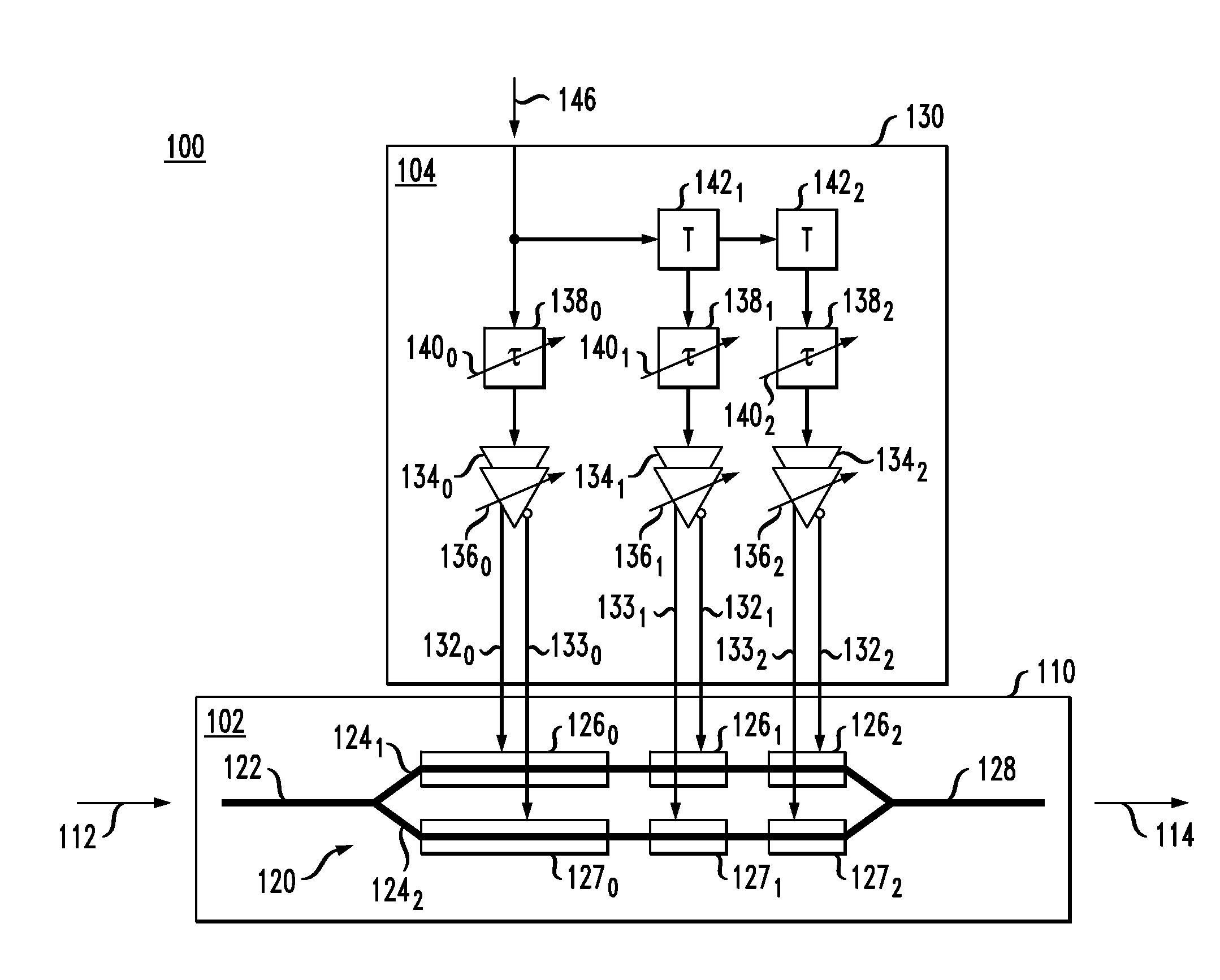
[0006]Disclosed herein are various embodiments of an opto-electronic circuit having an optical modulator and a driver circuit configured to generate a plurality of electrical drive signals for the optical modulator in a manner that causes the opto-electronic circuit to operate as a finite-impulse-response (FIR) filter. Different electrical drive signals generated by the driver circuit represent different taps of the FIR filter and are individually applied to different respective electrodes in the optical modulator without first being combined with one another prior to said individual application. The optical modulator represents an adder of the FIR filter and is configured to use the applied electrical drive signals to perform signal summation in the optical domain, thereby alleviating some of the limitations associated with the electrical RF circuitry used in the driver circuit. In various embodiments, the opto-electronic circuit can be employed in optical transmitters, equalizers,...


PUM


Abstract

We disclose an opto-electronic circuit having an optical modulator and a driver circuit configured to generate a plurality of electrical drive signals for the optical modulator in a manner that causes the opto-electronic circuit to operate as a finite-impulse-response (FIR) filter. Different electrical drive signals generated by the driver circuit represent different taps of the FIR filter and are individually applied to different respective electrodes in the optical modulator without first being combined with one another prior to said individual application. The optical modulator represents an adder of the FIR filter and is configured to use the applied electrical drive signals to perform signal summation in the optical domain, thereby alleviating some of the limitations associated with the electrical RF circuitry used in the driver circuit. The opto-electronic circuit can be employed in optical transceivers and equalizers and be configured to implement signal pre-emphasis, feed-forward equalization, or decision-feedback equalization.

Description

BACKGROUND[0001]1. Field[0002]The present disclosure relates to optical communication equipment and, more specifically but not exclusively, to light-modulating devices that can be used in optical transmitters and / or receivers.[0003]2. Description of the Related Art[0004]This section introduces aspects that may help facilitate a better understanding of the disclosure. Accordingly, the statements of this section are to be read in this light and are not to be understood as admissions about what is in the prior art or what is not in the prior art.[0005]Appropriate signal-processing methods can be used to enable optical transceivers implemented using silicon-based photonic integrated circuits (PICs) to work at bit rates that exceed the nominal limits imposed by carrier-recombination dynamics in the employed semiconductor material. For example, the pre-emphasis pulse-shaping technique can improve the inherent slow optical response of an electro-optic modulator using the rapid injection of...

Claims


Application Information

Patent Timeline
Patent Type & Authority Applications(United States)
IPC IPC(8): H04B10/2575H04B10/60H04B10/516
CPCH04B10/2575H04B10/60H04B10/516G02F1/225H04B10/5051G02F1/0121G02F1/0316G02F1/0327G02F2203/15G02F2203/585
Inventor LEE, SIAN CHONG J.AROCA, RICARDO A.SHAHRAMIAN, SHAHRIARDONG, PO
Owner ALCATEL LUCENT SAS
Why Eureka
Try Eureka