Transparent electrode, electronic device, and organic electroluminescent element
a technology of electronic devices and electrodes, applied in the direction of layered products, transportation and packaging, chemistry apparatuses and processes, etc., can solve the problems of high material costs, easy degradation of performance, and inability to lower driving voltage, etc., to achieve excellent conductivity, high optical transparency, and excellent conductivity
- Summary
- Abstract
- Description
- Claims
- Application Information
AI Technical Summary
Benefits of technology
Problems solved by technology
Method used
Image

Examples
examples
[0324]Hereinafter, one or more embodiments of the invention are detailed with Examples. However, the present invention is not limited thereto. Note that “%” used in Examples stands for “mass % (percent by mass)” unless otherwise specified.
first example
Production of Transparent Electrodes 1-1 to 1-17
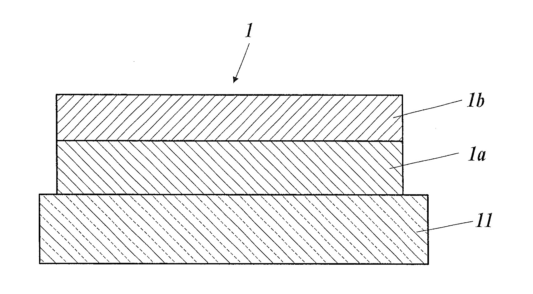
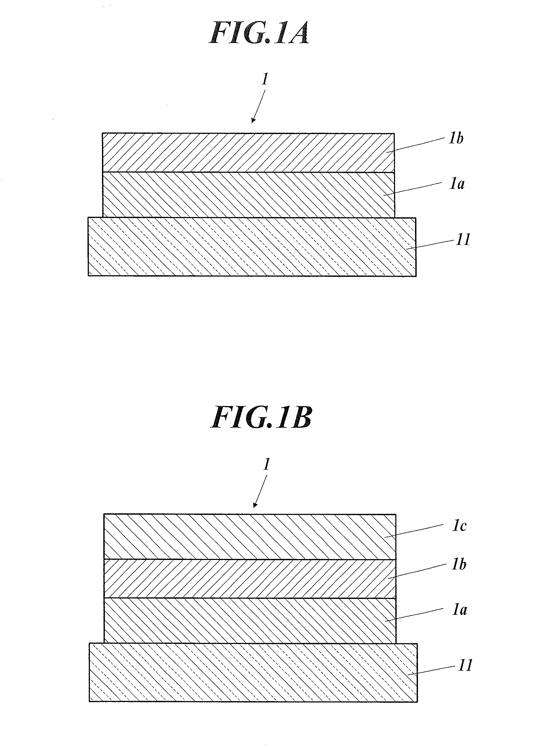
[0325]By the method described below, transparent electrodes of 1-1 to 1-17 were each produced in such a way that the area of a conductive region was 5 cm×5 cm. The transparent electrodes 1-1 to 1-4 were each produced as a transparent electrode having a single-layer structure, and the transparent electrodes 1-5 to 1-17 were each produced as a transparent electrode having a multilayer structure of an intermediate layer and a conductive layer.
[0326][Production of Transparent Electrodes 1-1 to 1-4]
[0327]By the method described below, the transparent electrodes 1-1 to 1-4 each having a single-layer structure were produced as comparative examples. First, a base composed of transparent alkali-free glass was fixed to a base holder of a commercial vacuum deposition device, and the base holder was mounted in a vacuum tank of the vacuum deposition device. In addition, silver (Ag) was placed in a tungsten resistive heating board, and the heating b...
second example
Production of Luminescent Panels 1-1 to 1-17
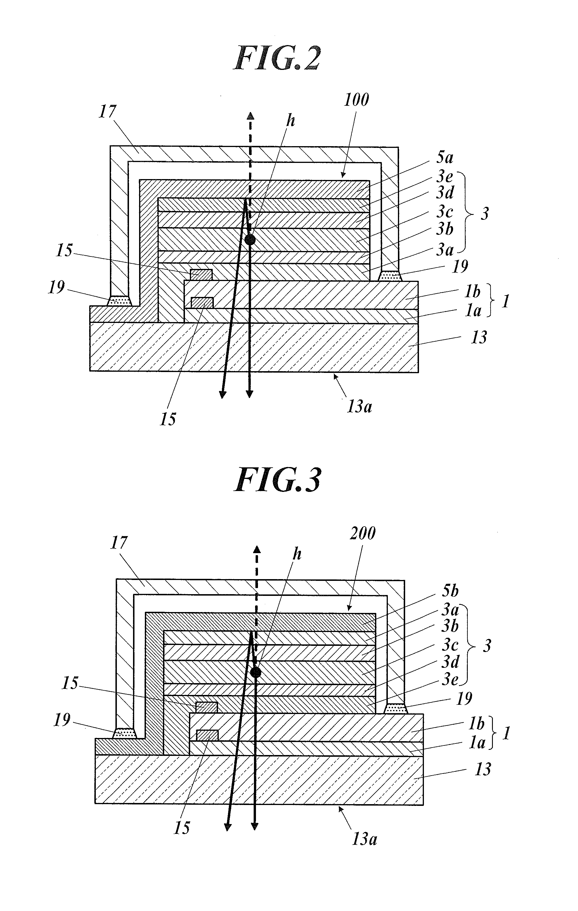
[0346]Top-and-bottom emission type organic EL elements respectively using, as anodes, the transparent electrodes 1-1 to 1-17 produced in First Example were produced. The procedure for producing them is described with reference to FIG. 6.
[0347]First, a transparent substrate 13 on which the transparent electrode 1 produced in First Example had been formed was fixed to a substrate holder of a commercial vacuum deposition device, and a vapor deposition mask was disposed in such a way as to face a formation face of the transparent electrode 1. Further, heating boards in the vacuum deposition device were filled with materials for respective layers constituting a light-emitting functional layer 3 at their respective amounts optimal to form the layers. The heating boards used were composed of a tungsten material for resistance heating.
[0348]Next, the pressure of a vapor deposition room of the vacuum deposition device was reduced to 4×10⁻⁴ Pa, and ...
PUM
| Property | Measurement | Unit |
|---|---|---|
| voltage | aaaaa | aaaaa |
| resistance | aaaaa | aaaaa |
| aromaticity | aaaaa | aaaaa |
Abstract
Description
Claims
Application Information
 - R&D Engineer
- R&D Manager
- IP Professional
- Industry Leading Data Capabilities
- Powerful AI technology
- Patent DNA Extraction
Browse by: Latest US Patents, China's latest patents, Technical Efficacy Thesaurus, Application Domain, Technology Topic.
© 2024 PatSnap. All rights reserved.Legal|Privacy policy|Modern Slavery Act Transparency Statement|Sitemap