Backside imaging through a doped layer

a layer and backside imaging technology, applied in the field of backthinning and backthinning of solid-state imaging sensors, can solve the problems of poor resolution, unsuitable non-coplanar surface, process steps, etc., and achieve the effect of uniformly maximizing the pixel fill factor, reducing the incidence of electron scattering, and improving the resolution

Active Publication Date: 2006-06-29
EOTECH LLC
View PDF22 Cites 204 Cited by
  • Summary
  • Abstract
  • Description
  • Claims
  • Application Information

AI Technical Summary

Benefits of technology

[0012] It is recognized that the only portion of the die that needs to be thinned in order to achieve good backside imaging performance is the backside surface region directly opposite the active pixel array. Accordingly, “area selective backside thinning” (ASBT) can be used to etch away the excess silicon from the backside of the die in the area of the active pixel array while the silicon underlying adjacent circuitry, bond pads and the periphery of the die is left thicker. The thicker layer, typically >25 microns thick, can be used to physically stabilize any unsupported portions of the membrane, thereby increasing device yield.
[0013] The selective thinning, herein described, deliberately excludes the black reference pixels from illumination by proximity focused electrons. In this way, the unthinned silicon can serve to shield the black reference pixels from both electron induced signal, which is induced primarily within the first 500 Å of silicon for a 2 keV electron, and most of the light induced signal. Due to the high level of electron bombarded gain, typically >100, this shielding is sufficient to allow the black reference pixels to serve their designated purpose for the targeted application.
[0016] ASBT represents an approach to improve thinning yield on backside thinned CMOS sensors. There is an alternative approach to improving thinning yield that is applicable to any area array image sensors independent of the type of image sensor architecture and regardless of whether or not ABST is employed. The approach employs a multiple stop layer structure. The simplest manifestation of this structure would consist of an I-P-I epitaxial structure on a standard P doped substrate as further elaborated below. This approach offers a number of distinct advantages over previously described etch stop techniques. First the use of a double stop layer improves thickness control. Second, terminating the etch leaving the P-doped layer relatively intact both increases the conductivity of the remaining epitaxy and isolates the passivation layer from the influences of the electric fields generated in the underlying circuitry. In practice this minimizes the appearance of dark current defects or “hot” pixels. A further refinement of this approach would be to add a doping ramp into the P-doped layer. This introduces a conductivity gradient “drift” region to introduce a small electric field to enhance conduction band electrons toward the collection node of the proximate pixel. Merely as an example, U.S. Pat. No. 3,631,303 at FIG. 4, details a III-V photocathode that uses a doping ramp to generate a drift field.
[0017] It should be noted that although designed for use in backthinned image arrays, the ramped structure will improve resolution on frontside illuminated devices particularly in the red where photons are absorbed deep within the silicon, U.S. Pat. No. 4,348,690 describes this advantage. The doping gradient employed in U.S. Pat. No. 4,348,690 varies within the range 1014 to 1016 dopant atoms / cm3. This range of doping provides a sufficient built in gradient without compromising the silicon's minority carrier diffusion length. The minority carrier diffusion length of silicon falls as doping increases. At a P-doping level of 1016 silicon retains an electron diffusion length on the order of 500 microns. Consequently virtually no photo-electrons are lost within the 10 microns or so of gradient doped epitaxy. Peak doping at the 1016 level is unacceptable for electron bombarded active pixel array sensors. In such application, at a target operating voltage of (for example) 2 KeV, the peak in electron-hole pair generation occurs at a depth of just over 200 Angstroms. In order to collect these electrons the surface doping must overcome the depletion associated with surface charge. In order to overcome the surface depletion within 200 Angstroms, doping levels on the order of 1019 atoms per cubic centimeter are required. At 1019 doping levels, the diffusion length of electrons in silicon is only a few microns. Consequently, to optimize the overall collection efficiency of an electron bombarded sensor, a more complex ramp is required which is characterized by a very high dopant concentration very close to the surface of incidence. The required ramp will achieve a surface doping concentration of at least 5×10¹⁸ atoms per cubic centimeter but drop to below 1×10¹⁸ atoms per cubic centimeter within the first micron of the surface. The balance of the gradient may then decline to dopant concentration levels similar to prior art, yielding a composite gradient, which may be characterized, as a whole, to be non-linear.

Problems solved by technology

This approach replaces metal shield patterning photolithographic process steps, which are not well suited to non-coplanar surfaces such as those generated by ASBT.
Secondary / backscattered electrons arising from the interaction with the anode of the (primary) proximity focused photoelectrons would ordinarily be accelerated along trajectories back to the pixel array, contributing signal to pixels other than that pixel to which the original primary electron was directed, thus contributing to halo, poor resolution, etc.

Method used


Image

  • Backside imaging through a doped layer
  • Backside imaging through a doped layer
  • Backside imaging through a doped layer

Examples


Embodiment Construction

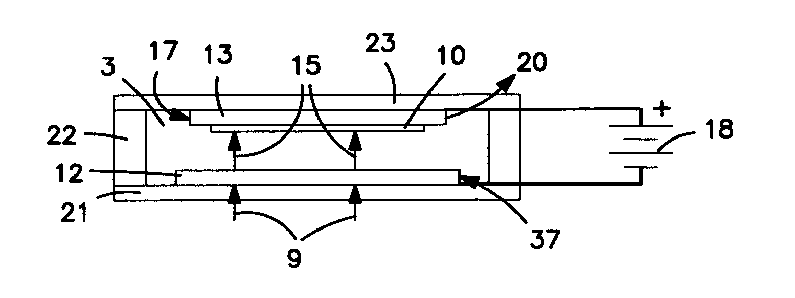
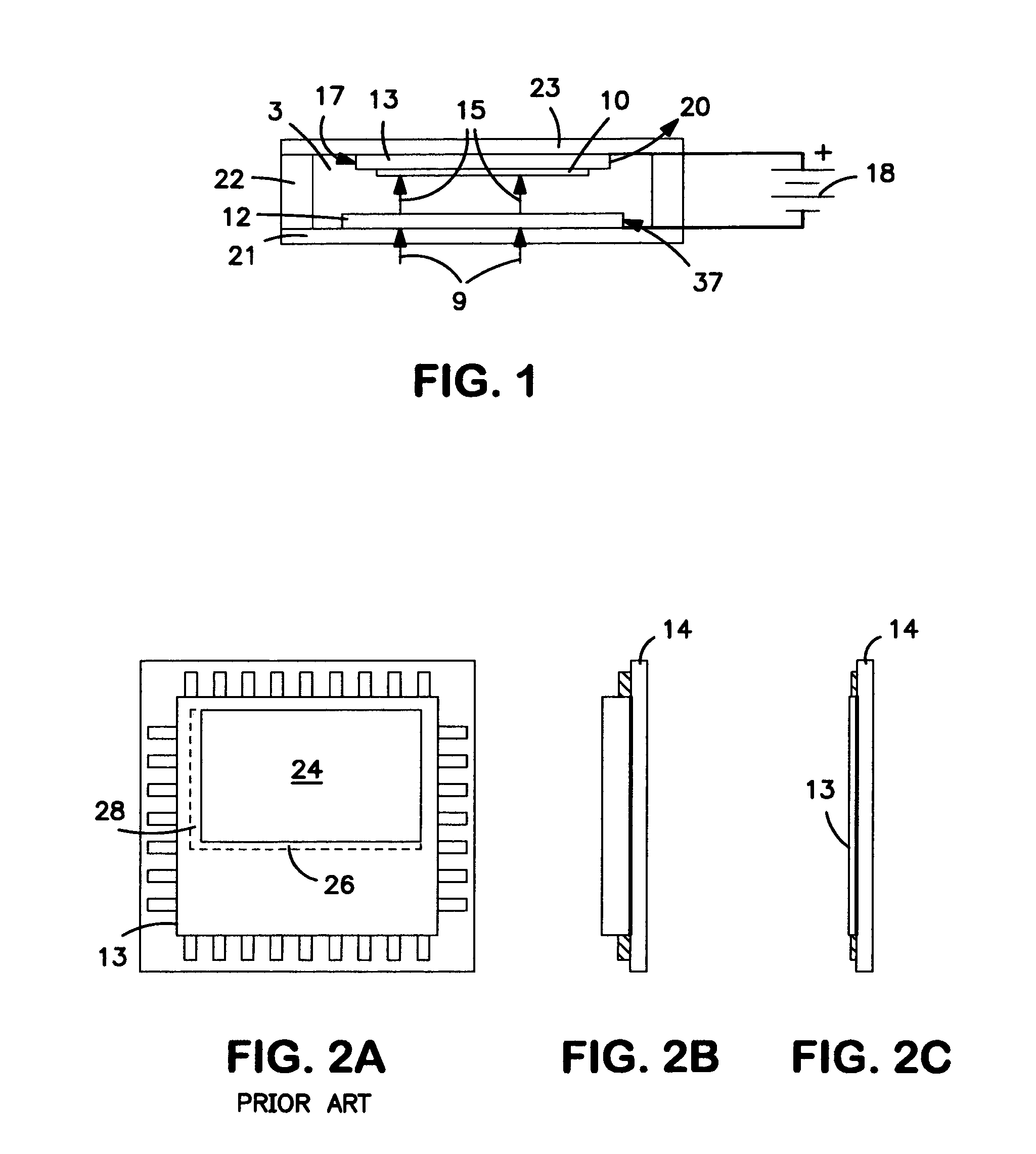
[0028] The context of the invention is illustrated in FIG. 1 where there is shown an example of an electron bombarded active pixel array component including a vacuum enclosure 3 which houses a photocathode 12 such as a GaAs, an InP / InGaAs, a transferred electron photocathode, or a multi-alkali photocathode, in proximity focus with a specialized active pixel array sensor chip 13 which forms the anode for receiving the proximity focused photoelectrons from photocathode 12 to which an acceleration voltage 37 is applied. In accordance with this invention the active pixel array sensor 13 is mounted with its backside 10 facing the photocathode 12. Photoelectrons 15 are emitted from photocathode 12 in response to incident light illustrated as arrows designated 16. Optical components, not shown, are typically employed to form an optical image on the photocathode. Any projection system may be used to place an image on the photocathode.

[0029] The photoelectrons 15 are accelerated by an appli...


PUM


Abstract

Backthinning in an area selective manner is applied to CMOS imaging sensors 12 for use in electron bombarded active pixel array devices. A further arrangement results in an array of collimators 51 aligned with pixels 42 or groups of pixels of an active pixel array providing improved image contrast of such image sensor. Provision of a thin P-doped layer 52 on the illuminated rear surface provides both a diffusion barrier resulting in improved resolution and a functional shield for reference pixels. A gradient in concentration of P-doped layer 52 optimizes electron collection at the pixel array.

Description

RELATED APPLICATIONS [0001] This application is a continuation-in-part of U.S. Ser. No. 10 / 355,8388, filed Jan. 31, 2003.FIELD OF THE INVENTION [0002] The invention relates to backthinned and backthinning of solid state imaging sensors. BACKGROUND OF THE INVENTION [0003] Focal plane imaging sensors are well known for the purpose of acquiring an electronic image from a sensor array implemented on a semiconductor die. Particularly widely used such devices include the CMOS imaging array (hereafter, CMOS imager) and the charge coupled device (hereafter, CCD). It is known in prior art to remove material from the backside of substrates, particularly for CCD applications. [0004] Focal plane imaging sensors can be backthinned for a number of reasons. Performance advantages of backthinned sensors can include improved light sensitivity as a result of improved effective fill factor. When properly passivated by a method such as that described in U.S. Pat. No. 5,688,715, backthinned CMOS sensors...

Claims


Application Information

Patent Timeline
Patent Type & Authority Applications(United States)
IPC IPC(8): H01J40/00H01LH01L21/00H01L27/146H01L29/04H01L29/06H01L31/00H01L31/062H01L31/113
CPCH01L27/14603H01L27/14623H01L27/1464H01L27/14643H01L27/14629H01L27/14625
Inventor COSTELLO, KENNETH A.FAIRBAIRN, KEVIN P.BROWN, DAVID W.CHUNG, YUNGOBER, PATRICIAYIN, EDWARD
Owner EOTECH LLC
Why Eureka
Try Eureka