Imaging device, signal processing method on solid-state imaging element, digital camera and controlling method therefor and color image data generating method

a solid-state imaging element and image processing technology, applied in the direction of radio frequency controlled devices, instruments, television systems, etc., can solve the problems of reducing the sensitivity or the s/n ratio of the signal obtained from the photoelectric conversion element in the lower portion, reducing the degree of blurring, and enhancing resolution

Inactive Publication Date: 2006-06-08
FUJIFILM CORP +1
View PDF19 Cites 59 Cited by
  • Summary
  • Abstract
  • Description
  • Claims
  • Application Information

AI Technical Summary

Benefits of technology

[0096] In accordance with the aforementioned signal processing method on solid-state imaging element, in the case of still image picture-taking, the weighting coefficient of the corresponding pixel is predetermined greater than that of the surrounding pixels to reduce the degree of blurring. In the case of animation picture-taking, the difference between the weighting coefficient of the corresponding pixel and the weighting coefficient of the surrounding pixels is predetermined small to raise the degree of blurring. In this arrangement, in the case of still image picture-taking, substantial addition of pixels is inhibited to enhance resolution. In the case of animation picture-taking, substantial addition of pixels is effected to reduce the number of pixels per frame, making it possible to perform high speed processing.
[0097] In accordance with the aforementioned digital camera controlling method, imaging is effected according to a signal processing method on solid-state imaging element, making it possible to optimize the imaging performance of the digital camera according to the purpose.
[0098] In accordance with the invention, even when the brightness of the object to be picture-taken is low, S / N ratio of pixel signal can be enhanced while inhibiting the deterioration of visual color resolution. In this manner, the sensitivity balance of photoelectric conversion portions of various hues can be enhanced, making it possible to enhance image quality and sensitivity. Accordingly, even when the photoelectric conversion portion is a laminated solid-state imaging element, there occurs no deterioration of image quality due to the reduction of the amount of light that reaches the underlying photoelectric conversion portions. Further, even when the photoelectric conversion portion is a multi-plate solid-state imaging element, arrangement can be made such that the properties of the various photoelectric conversion portions can be exhibited without any waste. By selectively or automatically predetermining the processing of charges in the photoelectric conversion portions with a plurality of pixels with respect to light rays other than G light according to the picture-taking conditions, etc., an image data having a quality desired by the user can be formed.

Problems solved by technology

It is thus disadvantageous in that the properties of the photoelectric conversion layer formed earlier are deteriorated by the heat used during the formation of contact wiring.
It is thus disadvantageous in that the amount of signal charges generated in the photoelectric conversion layers in the upper portion per constant amount of incident light rays is greater than the amount of signal charges generated in the photoelectric conversion elements in the lower portion per constant amount of incident light rays, causing the dispersion of sensitivity or the deterioration of S / N ratio of signals obtained from the photoelectric conversion elements in the lower portion (Problem 1).
In addition, in the aforementioned hybrid type solid-state imaging element, three color R, G and B signals constituting one-pixel data in color image data cannot be obtained from the same position.
Therefore, there occurs a problem that false colors become remarkable (Problem 2).
However, the technical progress of CCD type image sensors and CMOS type images has been almost limited.
Therefore, they types of image sensors face a problem of poor yield in production.
Further, the upper limit of the amount of photocharge that can be accumulated in one fine light-receiving portion is as low as about 3,000 electrons, with which 256 gradations can be difficultly expressed completely.
Therefore, it has been difficult to expect CCD type or CMOS type image sensor capable of outputting a higher quality from the standpoint of image quality or sensitivity.
Further, the S / N ratio of signal is lowered, deteriorating image quality.
Accordingly, in order to enhance image quality, it is separately necessary that the sensitivity of the lower layers be raised, unavoidably causing cost rise.
Accordingly, it cannot be freely selected which should be considered important color resolution or S / N ratio according to the picture-taking purpose or the object to be picture-taken, making it impossible to optimize the picture-taking conditions flexibly for the scene to be picture-taken.
In this type of a solid-state imaging element, it is difficult to uniform the sensitivity characteristics of the various hue photoelectric conversion layers.
Therefore, the sensitivity adjustment cannot be made unless the materials to be used or the layer formation conditions are changed.
Accordingly, when a photoelectric conversion layer for a specific hue can be made of a high sensitivity material, but other hue photoelectric conversion layers must be made of a relatively low sensitivity material, the performance of the element is predetermined on the basis of the low sensitivity material, making it impossible for the element to sufficiently exhibit the properties of the high sensitivity material.

Method used


Image

  • Imaging device, signal processing method on solid-state imaging element, digital camera and controlling method therefor and color image data generating method
  • Imaging device, signal processing method on solid-state imaging element, digital camera and controlling method therefor and color image data generating method
  • Imaging device, signal processing method on solid-state imaging element, digital camera and controlling method therefor and color image data generating method

Examples


embodiment 1-1

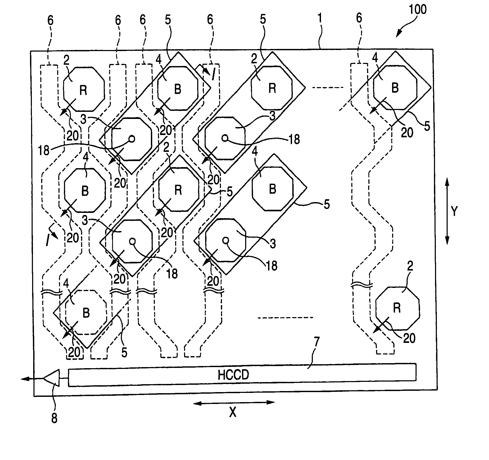
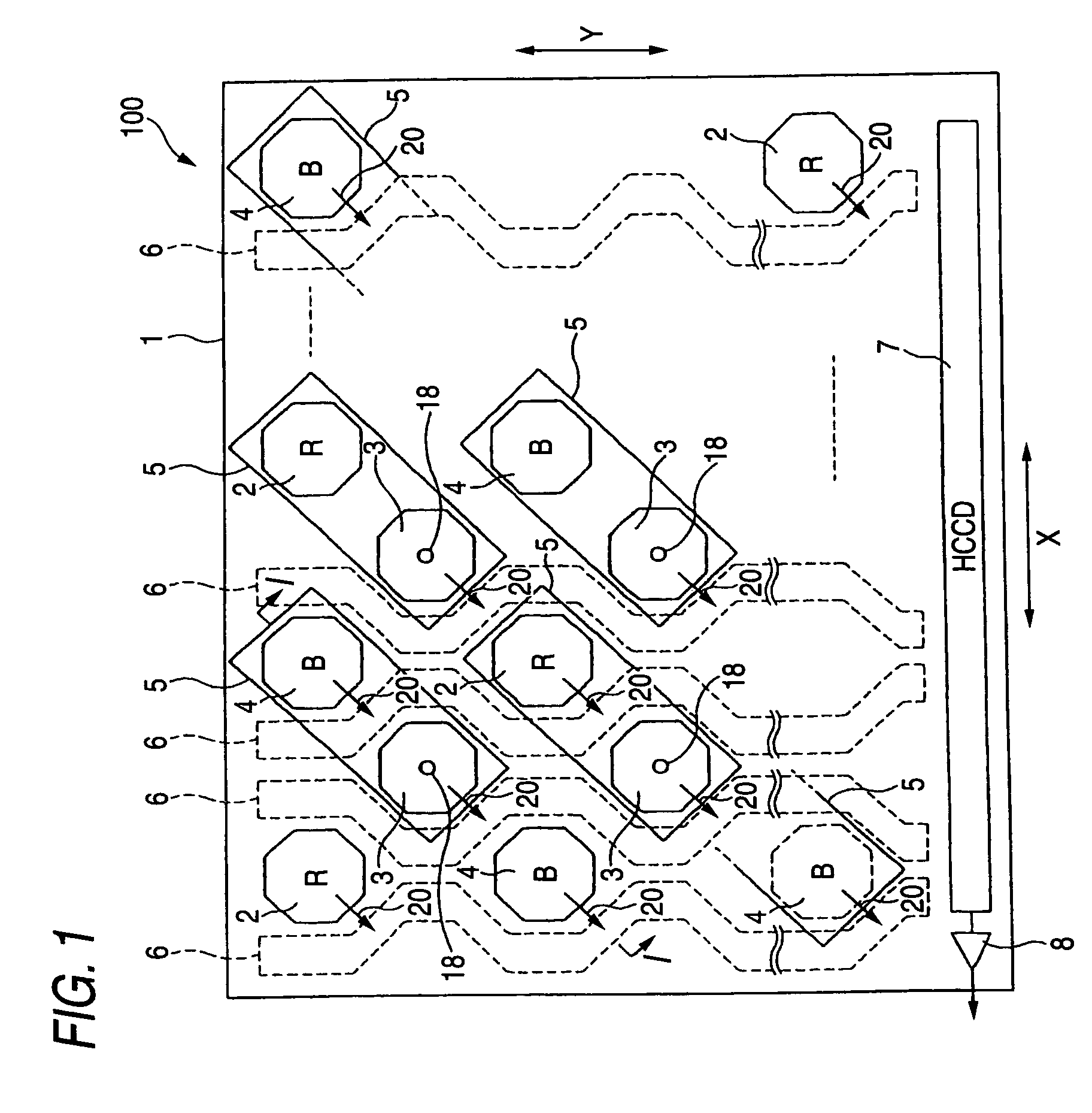
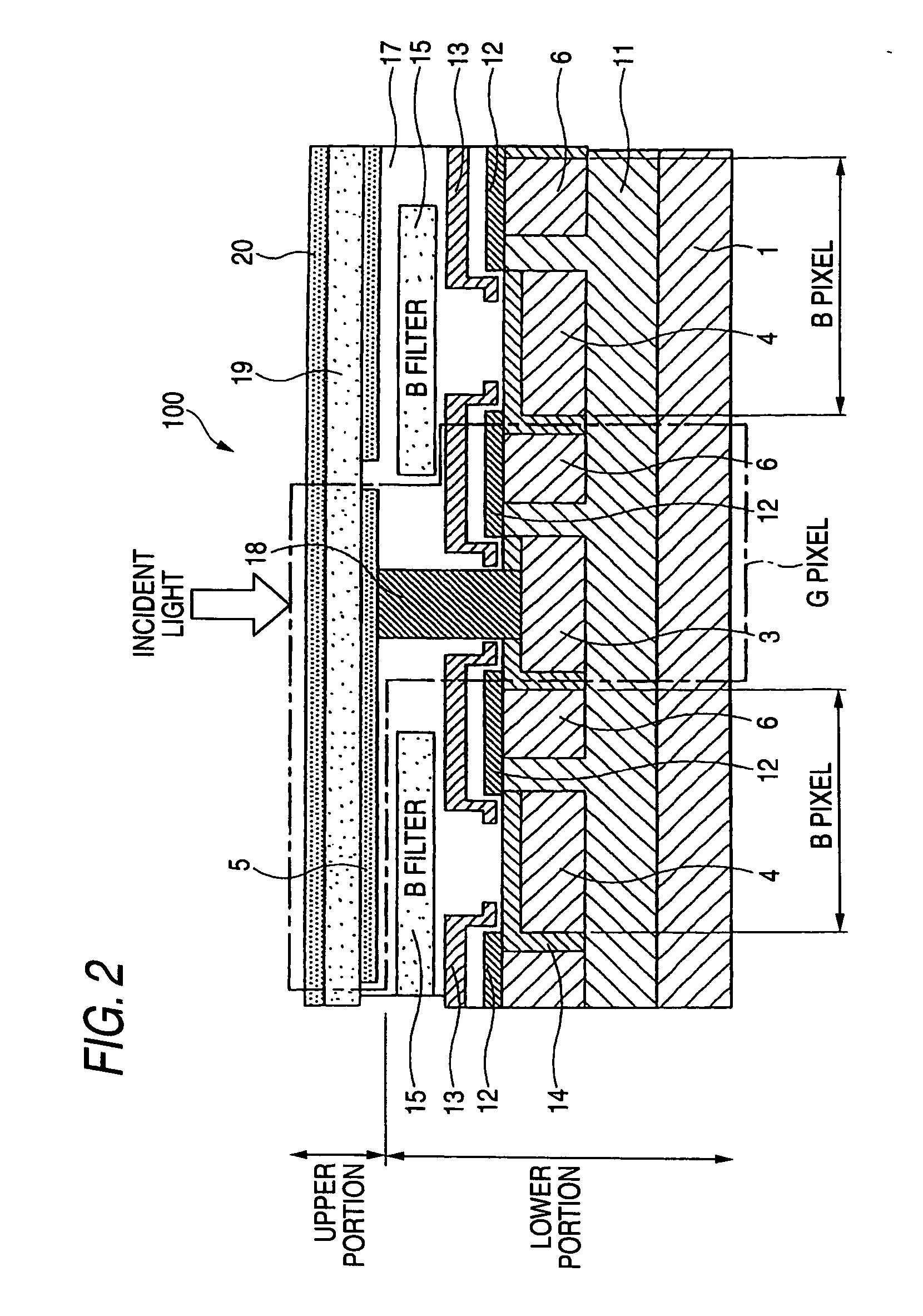
[0132]FIG. 1 is a diagrammatic plan view of a solid-state imaging element 100 for explaining an embodiment 1-1 of implementation of the invention. FIG. 2 is a diagrammatic sectional view taken on line I-I of FIG. 2.

[0133] On the surface portion of a semiconductor substrate 1 are aligned a plurality of photoelectric conversion elements 2, 4 made of silicon and a plurality of signal charge accumulating portions 3 in the line direction (X direction in FIG. 1) and in the row direction (Y direction in FIG. 1), respectively. In the present embodiment, the total number of the photoelectric conversion elements 2 and 4 is predetermined to be the same as the number of the signal charge accumulating portions 3. The number of the signal charge accumulating portions 3 is the same as the maximum number of pixel data in color image data that can be generated on the basis of a color signal obtained from the solid-state imaging element 100.

[0134] As shown in FIG. 1, in each odd line, a plurality o...

embodiment 1-2

[0219] As shown in FIG. 1, as green signals there are outputted those corresponding to the total number of pixel data in color image data. However, in the case of a solid-state imaging element which doesn't output as red signals and blue signals those corresponding to the total number of pixel data in color image data, red signals and blue signals are interpolated, making it likely that false colors can be generated. The present embodiment will be described hereinafter with reference to signal processing capable of inhibiting the generation of these false colors. This signal processing is executed in the digital signal processing portion 36 or analog signal processing 32 shown in FIG. 7.

[0220] The signal processing will be described hereinafter with reference to color signal obtained from three rows and three lines, totaling 9, of photoelectric conversion elements mainly composed of a photoelectric conversion element 2 or 4 corresponding to one-pixel data in color image data and co...

embodiment 2

[0251] Preferred embodiments of implementation of the imaging device, signal processing method on solid-state imaging element according to the invention and digital camera and its controlling method will be described in connection with the attached drawings.


PUM


Abstract

An imaging device for imaging an object to generate a color image data, comprising: a solid-state imaging element comprising: a photoelectric conversion layer laminated above a semiconductor substrate; photoelectric conversion elements comprising at least two kinds of photoelectric conversion elements aligned on the semiconductor substrate for detecting colors different from that to be detected by the photoelectric conversion layer; and a signal reading circuit formed on the semiconductor substrate for reading out color signals according to signal charge accumulated in the photoelectric conversion elements and signal charge generated in the photoelectric conversion layer; and a color signal generating unit for generating a color signal constituting one-pixel data in the color image data on the basis of signal charge accumulated in a first photoelectric conversion element corresponding the one-pixel data among the photoelectric conversion elements and signal charge accumulated in at least one second photoelectric conversion element, adjacent to the first photoelectric conversion element, for detecting the same color as that of the first photoelectric conversion element.

Description

BACKGROUND OF THE INVENTION [0001] 1. Field of the Invention [0002] The present invention relates to an imaging device which takes a picture of an object to generate a color image data. The present invention relates to a color image data generating method which generates a color image data from at least three color signals obtained by imaging an object. [0003] The present invention relates to an imaging device having a solid-state imaging element which comprises a plurality of photoelectric conversion layers each having a plurality of pixels and reads a signal charge out of the pixels in the photoelectric conversion layers as a pixel signal, a signal processing method on solid-state imaging element, a digital camera and a controlling method therefor. [0004] 2. Description of the Related Art [0005] As a solid-state imaging element free of color filter there has heretofore been proposed, e.g., laminated solid-state imaging element disclosed in JP-A-2002-83946. This laminated solid-st...

Claims


Application Information

Patent Timeline
Patent Type & Authority Applications(United States)
IPC IPC(8): H04N5/335G02B3/00H01L27/148H04N5/3722H04N9/04
CPCH04N5/335H04N9/045H01L27/14621H01L27/14627H01L27/14645H01L27/14623H04N25/00H04N23/843H04N25/134
Inventor INUIYA, MASAFUMI
Owner FUJIFILM CORP
Why Eureka
Try Eureka