Power Semiconductor Device of Stripe Cell Geometry

a technology of stripe cell and power semiconductor, applied in the direction of semiconductor devices, electrical devices, transistors, etc., can solve the problem that the performance of power semiconductor devices will be poor

Active Publication Date: 2015-11-26
UPI SEMICON CORP
View PDF3 Cites 2 Cited by
  • Summary
  • Abstract
  • Description
  • Claims
  • Application Information

AI Technical Summary

Benefits of technology

[0022]The advantage and spirit of the invention may be understood by the following detailed descriptions together with the appended drawings.

Problems solved by technology

There are different distances t1 and t2 between the ends of the striped body-doped regions 14 and adjacent doped regions 24; therefore, the distribution of the electrical field around the active area A1 will be non-uniform and the performance of the power semiconductor device will become poor.

Method used


Image

  • Power Semiconductor Device of Stripe Cell Geometry
  • Power Semiconductor Device of Stripe Cell Geometry
  • Power Semiconductor Device of Stripe Cell Geometry

Examples


first embodiment

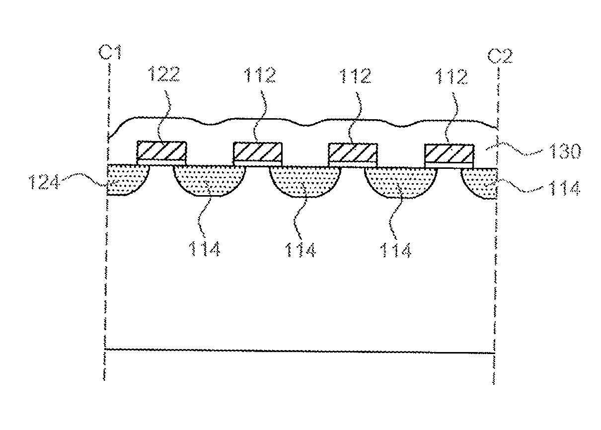
[0031]Please refer to FIG. 2A, FIG. 2B, FIG. 2C, FIG. 2D, and FIG. 2E. FIG. 2A, FIG. 2B, FIG. 2C, FIG. 2D, and FIG. 2E illustrate the power semiconductor device in the invention. This power semiconductor device is configured in a striped structure. FIG. 2A illustrates the configuration of a gate metal pad G and a source metal pad S on a surface of the power semiconductor device; FIG. 2B illustrates a top view of a striped cell structure in an active area A1 of the power semiconductor device; FIG. 2C and FIG. 2D illustrate cross-sections corresponding to the C1-C2 hatch and the C3-C4 hatch in FIG. 2B; FIG. 2E illustrates the distribution of a body-doped region 114 in the active area A1 of the power semiconductor device of this embodiment.

[0032]As shown in FIG. 2A, FIG. 2B, FIG. 2C, FIG. 2D, and FIG. 2E, this power semiconductor device includes a substrate 20, striped power semiconductor cells, and a guard ring structure 10. The active area A1 and a termination area A2 are defined on ...

second embodiment

[0038]FIG. 3A illustrates the power semiconductor device of the invention. Different from the gate metal pad 142 of FIG. 2A located at one side of the active area A1, the gate metal pad 242 of FIG. 3A extends inward from the center of one side of the termination area A2. The gate metal pad 242 is disposed above the striped gate conductive structures 212 and the ring-shaped conductive structures 222, and the gate metal pad 242 is electrically connected to the striped gate conductive structures 212 and the ring-shaped conductive structures 222 through the contact windows 232.

third embodiment

[0039]FIG. 3B illustrates the power semiconductor device of the invention. In this embodiment, two adjacent striped gate conductive structures 312 are connected through a vertical connection structure 313 to form a C-shaped conductive structure. The configuration of the gate metal pad 342 shown in FIG. 3B is similar with the configuration of the gate metal pad 142 shown in FIG. 2A. However, the gate metal pad 342 is electrically connected to one end of the C-shaped conductive structure and the ring-shaped conductive structures 322 through the contact windows 332. Therefore, the gate metal pad 342 of FIG. 3B needs fewer contact windows 332 than the gate metal pad 142 of FIG. 2A.

[0040]FIG. 4A, FIG. 4B, and FIG. 4C illustrate three different embodiments of the configuration of the gate metal pad G and the source metal pad S on a surface of the power semiconductor device in the invention. In FIG. 4A, the gate metal pad G extends from the center of one side of the chip to opposite side o...


PUM


Abstract

A power semiconductor device of stripe cell geometry including a substrate, a plurality of striped power semiconductor units, and a guard ring structure is provided. The substrate has an active area and a termination area surrounding the active area defined thereon. The striped semiconductor unit includes a striped gate conductive structure. The striped semiconductor units are located in the active area. The guard ring structure is located in the termination area and includes at least a ring-shaped conductive structure surrounding the striped power semiconductor units. The ring-shaped conductive structure and the striped gate conductive structures are formed on the same conductive layer, and at least one of the striped gate conductive structures is separated from the nearby ring-shaped conductive structure and electrically connected to the nearby ring-shaped conductive structure through the gate metal pad.

Description

BACKGROUND OF THE INVENTION[0001]1. Field of the Invention[0002]The invention relates to a power semiconductor device; in particular, to a power semiconductor device of stripe cell geometry.[0003]2. Description of the Prior Art[0004]The power semiconductor device has become an important power control product due to its advantages of lower switching loss and simple driving circuit and rapid development of semiconductor manufacturing process technologies. The power semiconductor devices can be divided into trench gate power semiconductor devices and planar gate power semiconductor devices according to their different channel positions. The channel of the trench gate power semiconductor device is disposed along a direction vertical to the chip surface; the channel of the trench gate power semiconductor devices is disposed along a direction parallel to the chip surface. The power semiconductor devices can be also divided into squared cells and striped cells according to their different ...

Claims


Application Information

Patent Timeline
Patent Type & Authority Applications(United States)
IPC IPC(8): H01L29/06H01L27/088
CPCH01L29/0619H01L27/088H01L29/0692H01L29/0696H01L29/404H01L29/4238H01L29/7811H01L29/7813
Inventor TU, KAO-WAYTSAI, YI-YUNCHANG, YUAN-SHUN
Owner UPI SEMICON CORP
Why Eureka
Try Eureka