Integrated control for silicon photonics

a technology of integrated control and silicon photonics, applied in the field of telecommunication techniques, can solve the problems of serial link performance limited by the electrical bandwidth of the channel and the electronic components, and the large amount of bandwidth of the internet and mobile applications for transferring photos, video, music and other multimedia files

Active Publication Date: 2015-11-26
MARVELL ASIA PTE LTD
View PDF16 Cites 58 Cited by
  • Summary
  • Abstract
  • Description
  • Claims
  • Application Information

AI Technical Summary

Benefits of technology

[0005]The present invention relates to telecommunication techniques. More specifically, various embodiments of the present invention provide a communication interface that is configured to transfer data at high bandwidth over optical communication networks. In certain embodiments, the communication interface is used by various devices, such as spine switches and leaf switches, within a spine-leaf network architecture, which allows large amount of data to be shared among servers.

Problems solved by technology

But Internet and mobile applications continuously demand a huge amount of bandwidth for transferring photo, video, music, and other multimedia files.
Serial link performance is limited by the channel electrical bandwidth and the electronic components.
Stacking chips into so-called 3-D ICs promises a one-time boost in their capabilities, but it's very expensive.

Method used


Image

  • Integrated control for silicon photonics
  • Integrated control for silicon photonics
  • Integrated control for silicon photonics

Examples


Embodiment Construction

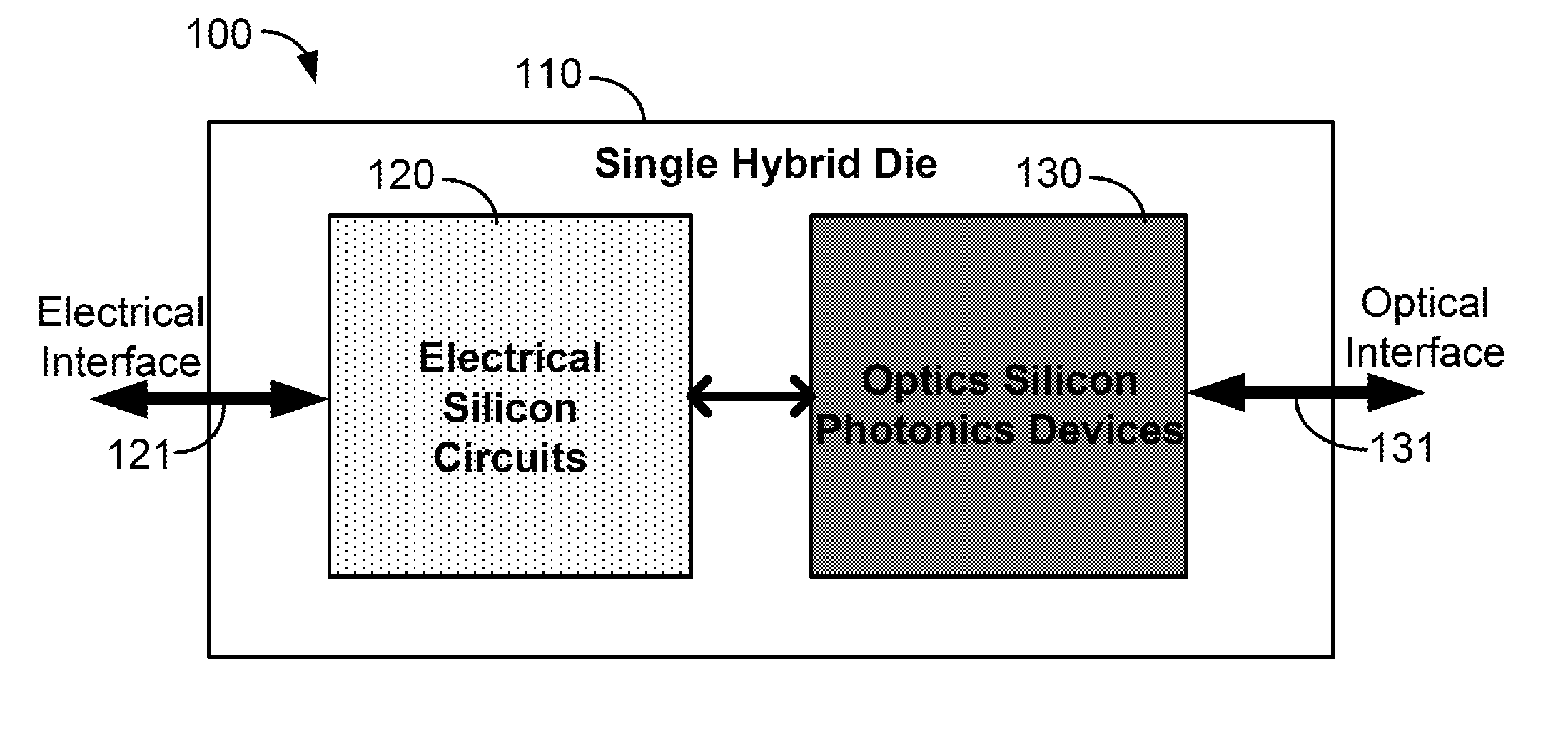
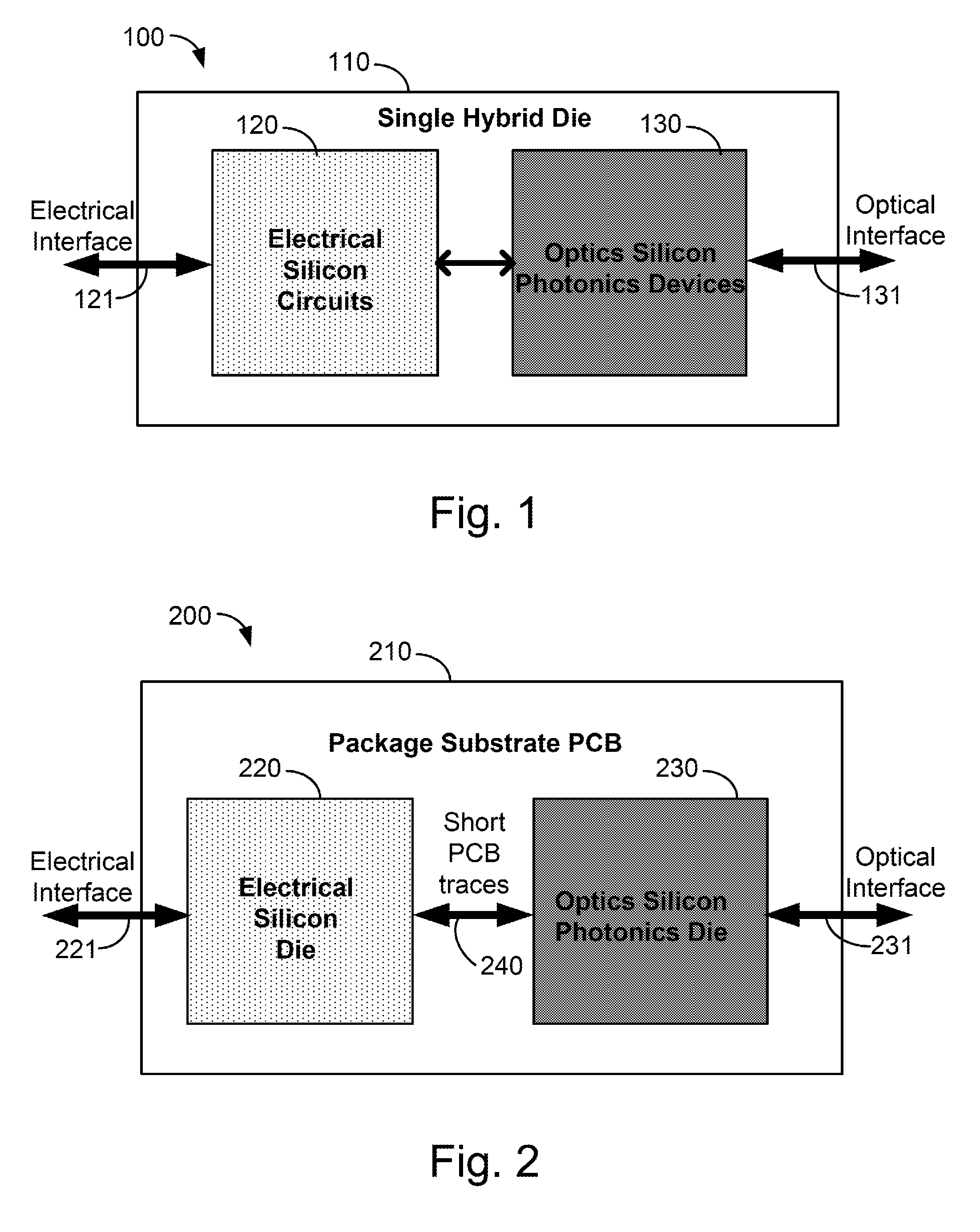
[0042]This present invention relates to telecommunication techniques. More specifically, various embodiments of the present invention provide a communication interface that is configured to transfer data at high bandwidth over optical communication networks. In certain embodiments, the communication interface is used by various devices, such as spine switches and leaf switches, within a spine-leaf network architecture, which allows large amount of data to be shared among servers.

[0043]In the last decades, with advent of cloud computing and data center, the needs for network servers have evolved. For example, the three-level configuration that have been used for a long time is no longer adequate or suitable, as distributed applications require flatter network architectures, where server virtualization that allows servers to operate in parallel. For example, multiple servers can be used together to perform a requested task. For multiple servers to work in parallel, it is often imperat...


PUM


Abstract

In an example, the present invention includes an integrated system on chip device. The device is configured on a single silicon substrate member. The device has a data input / output interface provided on the substrate member. The device has an input / output block provided on the substrate member and coupled to the data input / output interface. The device has a signal processing block provided on the substrate member and coupled to the input / output block. The device has a driver module provided on the substrate member and coupled to the signal processing block. In an example, the device has a driver interface provided on the substrate member and coupled to the driver module and configured to be coupled to a silicon photonics device. The device also has an interface configured to communicate between the silicon photonics device and the control block.

Description

CROSS-REFERENCE TO RELATED APPLICATIONS[0001]This application claims priority to and is a continuation of U.S. patent application Ser. No. 14 / 323,254, filed Jul. 3, 2014, which claims priority to U.S. Provisional Application No. 61 / 847,523, filed Jul. 17, 2013, and also claims priority to U.S. Provisional Application No. 61 / 873,784, filed Sep. 4, 2013, commonly assigned and incorporated by reference herein for all purposes.BACKGROUND OF THE INVENTION[0002]The present invention relates to telecommunication techniques. More particularly, the present invention provides an integrated electrical optics multiple chip module and methods.[0003]Over the last few decades, the use of communication networks exploded. In the early days Internet, popular applications were limited to emails, bulletin board, and mostly informational and text-based web page surfing, and the amount of data transferred was usually relatively small. Today, Internet and mobile applications demand a huge amount of bandwi...

Claims


Application Information

Patent Timeline
Patent Type & Authority Applications(United States)
IPC IPC(8): H04B10/70
CPCH04B10/70H04B10/801H01S5/0261H01S5/0427H04B10/07955H04J14/0221H04B10/5561H04L49/109H03L7/0807H03L2207/50H04B10/40H04B10/541
Inventor NAGARAJAN, RADHAKRISHNAN L.
Owner MARVELL ASIA PTE LTD
Why Eureka
Try Eureka