Pixel driving circuit and driving method thereof, and display device

a driving circuit and driving method technology, applied in the field of display technology, can solve the problems of affecting display quality, difficult to meet the requirements of thin and compact design of display devices, and high cost of sub-pixel driving chips, so as to reduce the number of gamma voltage supplies, improve display quality, and avoid large noise

Active Publication Date: 2015-12-10
BOE TECH GRP CO LTD
View PDF3 Cites 10 Cited by
  • Summary
  • Abstract
  • Description
  • Claims
  • Application Information

AI Technical Summary

Benefits of technology

[0020]The present invention provides a pixel driving circuit and a driving method thereof, and a display device, by performing source single-driving on sub-pixels by the sub-pixel driving chips which are provided opposite to each other, respectively, the used pins of the sub-pixel driving chip are reduced, advantageous effect of the present invention specifically includes:
[0021]I. pins occupied by the Gamma voltage supplies are reduced, thus the number of the Gamma voltage supplies is decreased, a large amount of noise is avoided, and the display quality is improved;
[0022]II. the number of the D/A converters o

Problems solved by technology

Since signal lines for Gamma voltage supplies are exposed outside, large number of Gamma voltage supplies may result in large amount of noise, which may affect the display quality.
In addition, the sub-pixel driving chip is expensive in cost, use of its pins should be saved as far as possibl

Method used


Image

  • Pixel driving circuit and driving method thereof, and display device
  • Pixel driving circuit and driving method thereof, and display device
  • Pixel driving circuit and driving method thereof, and display device

Examples


embodiment 1

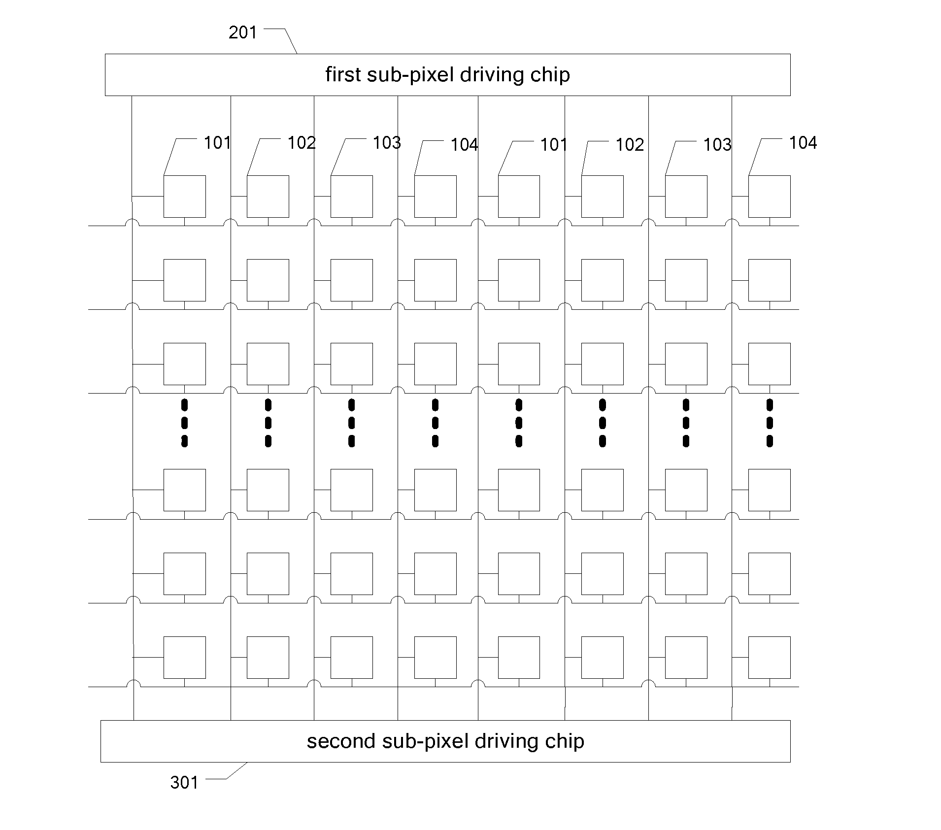
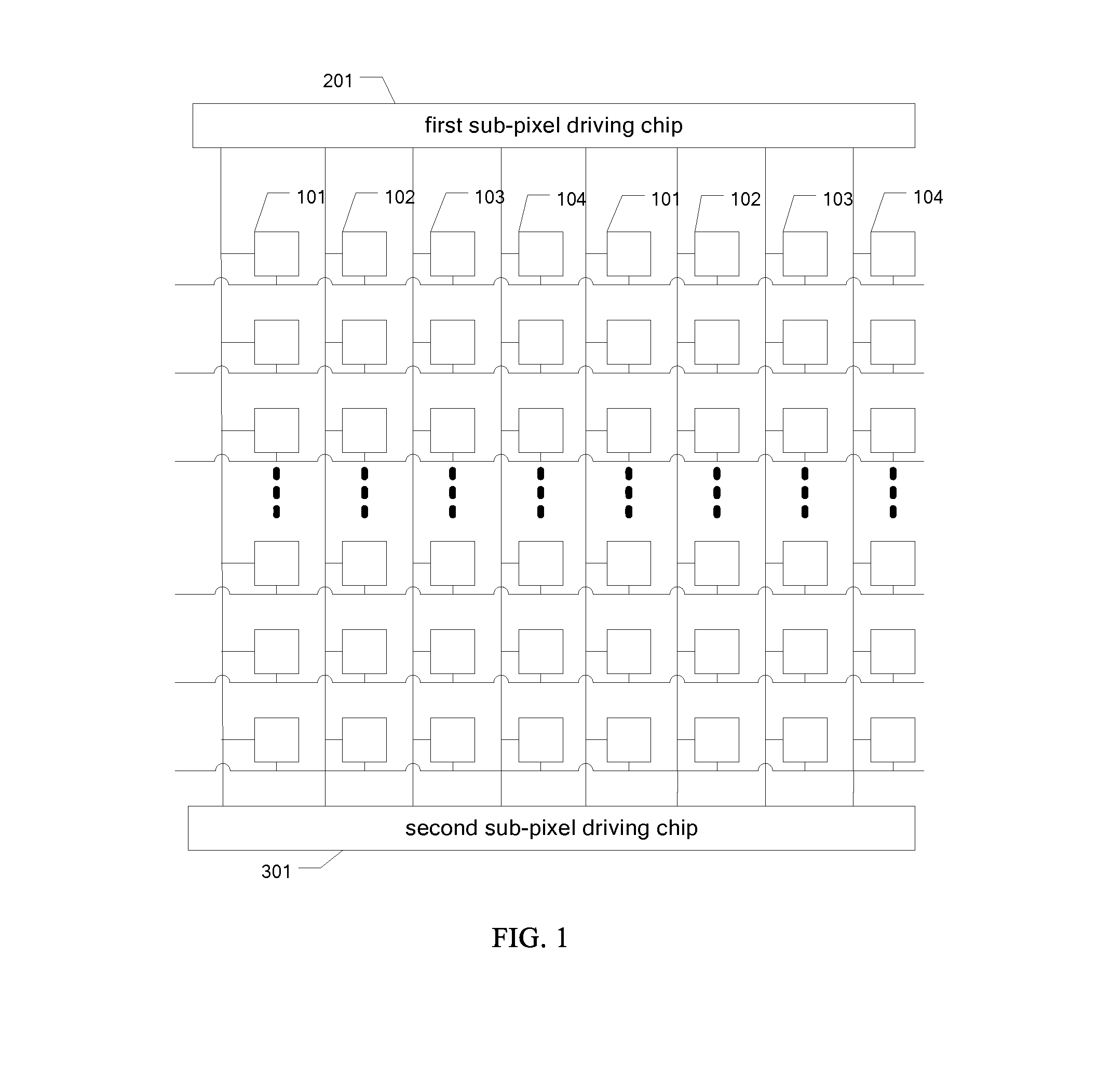
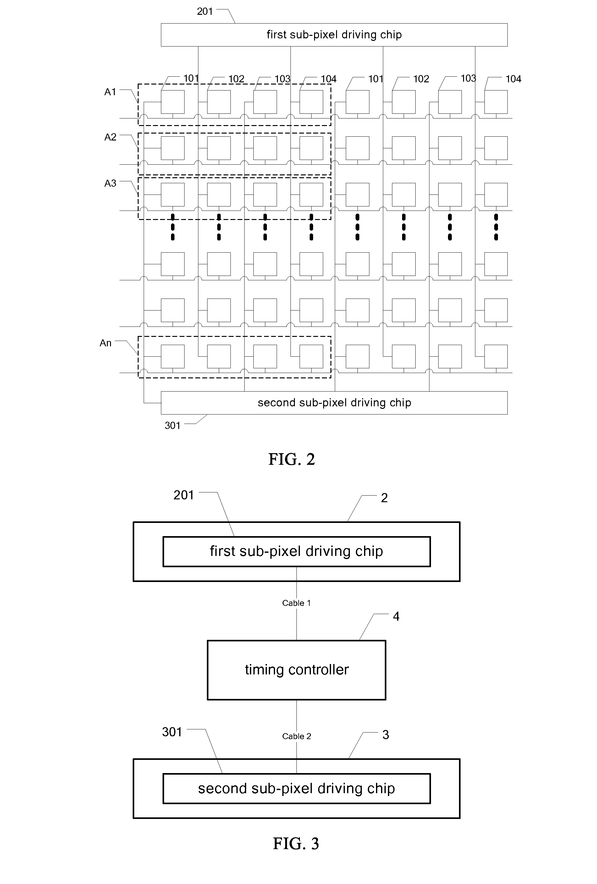
[0059]The pixel driving circuit in the embodiment 1 of the present invention is applied to a pixel array in a stripe arrangement manner, in which sub-pixels in each pixel are arranged in the same row. FIG. 4 is a structural schematic diagram of a pixel driving circuit in the embodiment 1 of the invention. As shown in FIG. 4, for example, four sub-pixels are arranged in one row in the order of red, green, blue and white so as to form a pixel 110. A first sub-pixel driving chip 201 is provided on a first driving circuit board 2, a second sub-pixel driving chip 301 is provided on a second driving circuit board 3, the first driving circuit board 2 is a X-direction circuit board and provided above the display screen of the display device, the second driving circuit board 3 is a X-direction circuit board and provided below the display screen of the display device. The green sub-pixel 102 and the white sub-pixel 104 are connected to the first sub-pixel driving chip 201 respectively, and th...

embodiment 2

[0064]The pixel driving circuit in the embodiment 2 is similar to that in the embodiment 1, difference between them is that the pixel driving circuit in the embodiment 2 is applied to a pixel array in a square (2×2 matrix) arrangement. FIG. 6 is a structural schematic diagram of the pixel driving circuit in the embodiment 2 of the present invention, as shown in FIG. 6, for example, in a pixel 110, the red sub-pixel 101 is located above the blue sub-pixel 103, the green sub-pixel 102 is located above the white sub-pixel 104, the red sub-pixel 101 and the green sub-pixel 102 are located at upper portion of the pixel, and the blue sub-pixel 103 and the white sub-pixel 104 are located at lower portion of the pixel. The green sub-pixel 102 and the white sub-pixel 104 are connected to the first sub-pixel driving chip 201 respectively, while the red sub-pixel 101 and the blue sub-pixel 103 are connected to the second sub-pixel driving chip 301 respectively. The first sub-pixel driving chip...


PUM


Abstract

The present invention provides a pixel driving circuit and a driving method thereof, and a display device. The pixel driving circuit is used for driving a pixel array, wherein each pixel in the pixel array comprises four sub-pixels with different colors, and wherein the pixel driving circuit comprises: at least one first sub-pixel driving chip and at least one second sub-pixel driving chip, wherein the at least one first sub-pixel driving chip each is connected to a part of sub-pixels corresponding thereto in corresponding pixels to drive them, and the at least one second sub-pixel driving chip each is connected to the other part of sub-pixels corresponding thereto in the corresponding pixels to drive them. In the invention, noise interference can be avoided, and the display quality is improved; the cost is reduced; signal transmitting efficiency is increased and the EMI characteristic of products is improved.

Description

FIELD OF THE INVENTION[0001]The present invention relates to the field of display technology, and particularly relates to a pixel driving circuit and a driving method thereof, and a display device.BACKGROUND OF THE INVENTION[0002]Design of modules of a display device adopting Active Matrix / Organic Light Emitting Diode (AMOLED) is quite complicated, and when a resolution of the display device is increased to more than 3840×2160 (large-size display), a design of four sub-pixels with different colors (that is, Red, Green, Blue and White, RGBW for short) is generally adopted. For the design of four sub-pixels with different colors, a gate / source double-driving method is generally used. FIG. 1 shows a schematic diagram of a driving circuit for four sub-pixels with different colors in the prior art, as shown in FIG. 1, the pixel driving circuit in the prior art comprises: a first driving circuit board, a second driving circuit board and a pixel array, wherein the first driving circuit boa...

Claims


Application Information

Patent Timeline
IPC IPC(8): G09G3/34G09G5/18G09G3/20G09G3/32
CPCG09G3/3413G09G3/3258G09G5/18G09G3/3266G09G2330/028G09G2300/0828G09G2300/0452G09G2320/0673G09G3/2074G09G3/3225G09G3/3648G09G2300/0426G09G2320/0223G09G2320/0276G09G2330/06G09G2310/0281
Inventor XIE, HONGJUN
Owner BOE TECH GRP CO LTD
Why Eureka
Try Eureka