Level shift circuit

a level shift and circuit technology, applied in the direction of logic circuit coupling/interface arrangement, pulse generator, pulse technique, etc., can solve the problems that the input of the rs flip-flop b, /b> is likely to be subjected to faulty noise operation, and achieve the effect of preventing a possible damage to a circuit element and preventing a possible faulty operation

Active Publication Date: 2015-12-10
SHARP KK
View PDF0 Cites 28 Cited by
  • Summary
  • Abstract
  • Description
  • Claims
  • Application Information

AI Technical Summary

Benefits of technology

[0030]In the level shift circuit having the aforementioned feature, when a high-side circuit configured by first and second load circuits and a comparator becomes in a floating state with respect to a reference voltage (ground voltage) of this level shift circuit and an output signal of the comparator shifts to a high level according to change in an input signal which is input to first and second current control elements, following the output level of the high-voltage circuit which is configured by a power switching element or the like driven by this output signal with an external bootstrap circuit, a high voltage supplied to the high-voltage circuit is applied to the high-side power source terminal to be level-shifted to a signal level needed for driving of this high-voltage circuit. Then, as a result of this level shift, a high voltage which is divided is to be applied also to each current ou...

Problems solved by technology

However, there is a problem that input of the RS flip-flop 34 is likely to be subjected to faulty operation with r...

Method used


Image

  • Level shift circuit
  • Level shift circuit
  • Level shift circuit

Examples


Embodiment Construction

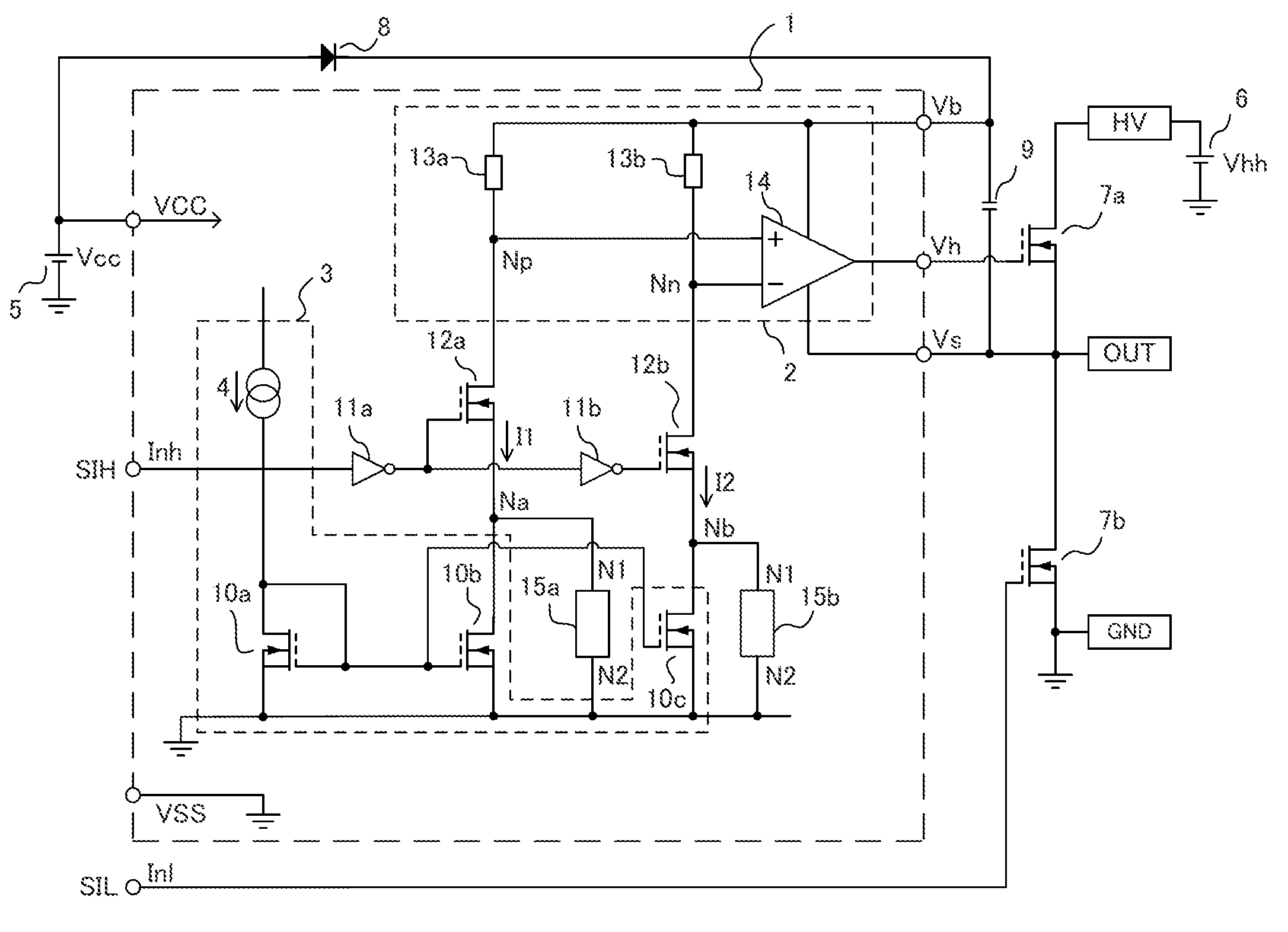
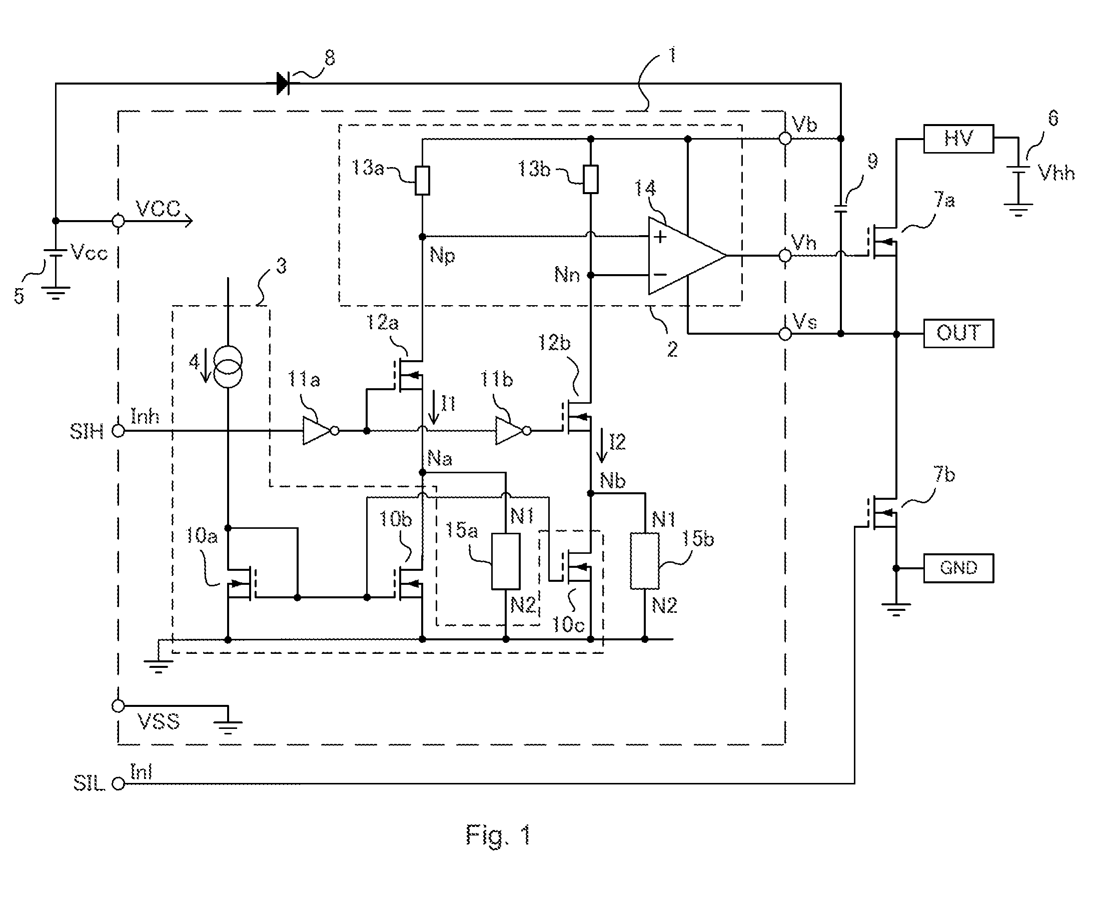
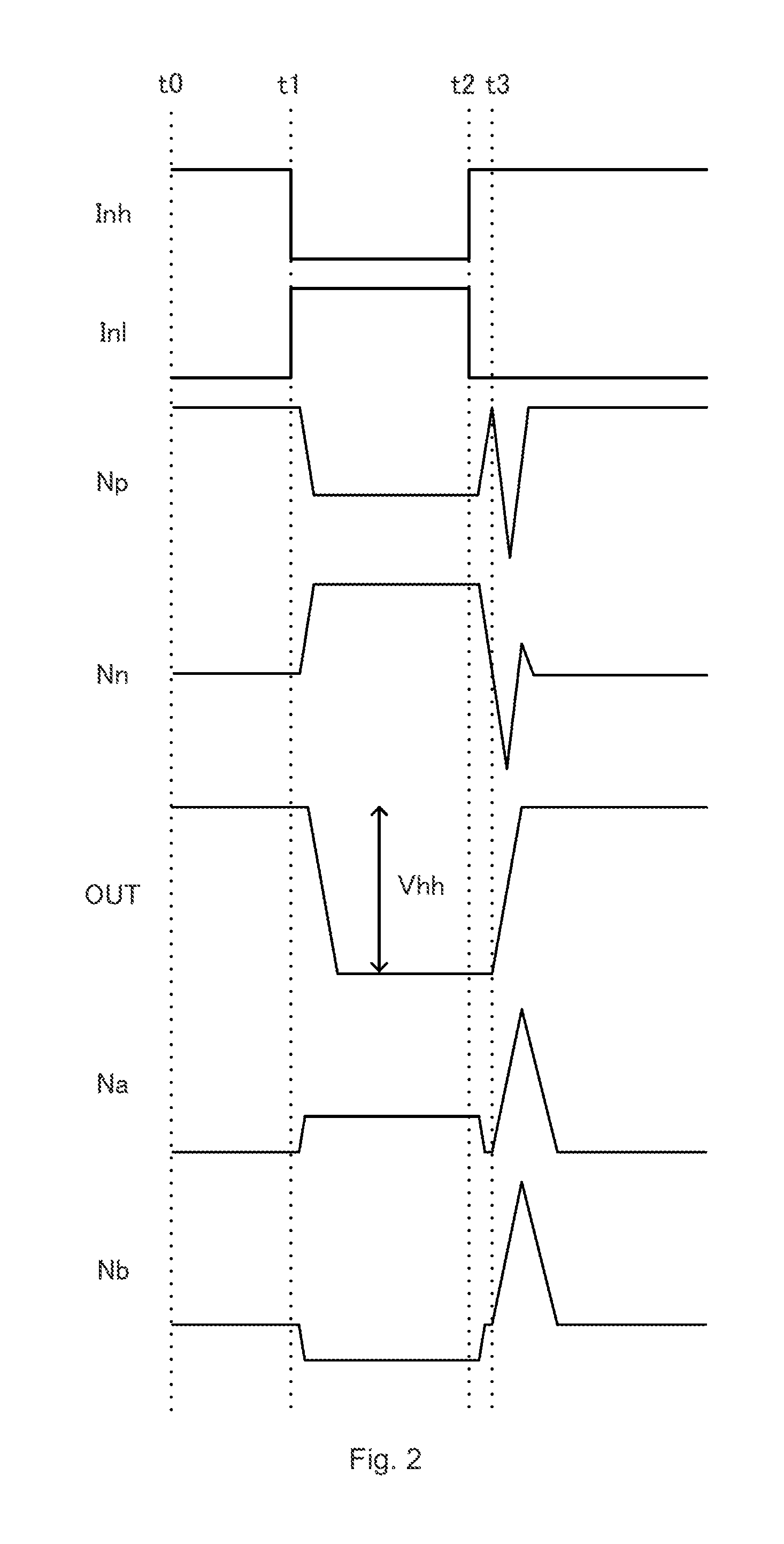
[0039]Description will be given below for a level shift circuit according to the present invention (hereinafter, referred to as “present invention circuit” as appropriate) with reference to drawings based on embodiments. Note that, in the present invention circuit described in each embodiment below, description will be given for elements in common with those of a conventional inverter circuit exemplified in FIG. 6 by giving same reference signs thereto even if having different names, in order to make the understanding of the description easier.

[0040]FIG. 1 shows one example of a circuit configuration of the present invention circuit. The present invention circuit 1 is configured by including a high-side circuit 2, a current generating circuit 3, two inverters 11a and 11b, a pair of n-type high voltage MOSFETs 12a and 12b (corresponding to first and second current control elements), a pair of voltage suppressing circuits 15a and 15b, n-type high voltage MOSFETs 7a and 7b, a diode 8 a...


PUM


Abstract

Provided is a high-reliability level shift circuit not prone to faulty operation due to noise. A level shift circuit 1 is provided with: first and second current control elements 12a and 12b into control terminals of which a reverse-phase input signal and an in-phase input signal are input, respectively; first and second load circuits 13a and 13b which are connected at one end to a high-side power source terminal Vb and at the other end to each of first terminals of the first and second current control elements 12a and 12b; a comparator 14 in which a pair of differential input terminals Np and Nn are connected separately to each of the first terminals of the first and second current control elements 12a and 12b; a current generating circuit 3 in which first and second current output terminals Na and Nb are connected to second terminals of the first and second current control elements 12a and 12b, and which separately generates a current which flows through the respective first and second current control elements 12a and 12b; and voltage suppressing circuits 15a and 15b which are connected separately or commonly to the first and second current output terminals Na and Nb, respectively, and suppress voltage from rising in the first and second current output terminals Na and Nb, respectively.

Description

TECHNICAL FIELD[0001]The present invention relates to a level shift circuit, and relates to a circuit that converts a voltage level of a control signal controlling a half-bridged switching element such as MOSFET, IGBT, SiCFET, or GaNFET, which is mainly used in an inverter circuit, to an appropriate level for the control.BACKGROUND ART[0002]An inverter system capable of high level control by a microcontroller has been widely used for controlling a motor which is used in household electrical appliances, such as an air conditioner or a refrigerator, in order to improve energy-saving performance. On the other hand, with practical use of a wide band gap semiconductor element such as SiCFET or GaNFET, application to an inverter circuit has been studied in an effort to aim efficiency improvement by low on-resistance and high frequency characteristics thereof.[0003]FIG. 6 shows an example of a circuit configuration of a conventional inverter circuit. FIG. 6 is an example of a configuration...

Claims


Application Information

Patent Timeline
IPC IPC(8): H03K3/356H03K19/0185
CPCH03K19/018507H03K3/356H03K19/00361H03K3/35613
Inventor KIHARA, SEIICHIRO
Owner SHARP KK
Why Eureka
Try Eureka