
Touch sensor integrated display device and method of manufacturing the same

a display device and touch sensor technology, applied in the field of display devices, can solve the problems of unsatisfactory display quality and touch accuracy, add thickness and weight to the display device, etc., and achieve the effects of increasing cstg, reducing unwanted load, and more accurate touch

Active Publication Date: 2015-12-31
LG DISPLAY CO LTD
View PDF12 Cites 63 Cited by
  • Summary
  • Abstract
  • Description
  • Claims
  • Application Information

AI Technical Summary

Benefits of technology

This patent text describes a display device with advanced touch sensing technology. The device uses multi-purpose elements to operate both the display pixels and sense user inputs, resulting in a thinner and lighter device with improved optical performance. The improved configuration also allows for more accurate touch detection at the edges of the display and reduces unwanted load on the touch driving electrode while suppressing light leakage and color mixing.

Problems solved by technology

However, overlaying such a separate capacitive touch sensor panel can add thickness and weight to the display device.
In such an In-Cell type touch enabled display device, the integrated touch screen components may have a relatively high resistance and / or may capacitively couple to other display components, leading to unsatisfactory display quality and touch accuracy.

Method used


Image

  • Touch sensor integrated display device and method of manufacturing the same
  • Touch sensor integrated display device and method of manufacturing the same
  • Touch sensor integrated display device and method of manufacturing the same

Examples


Embodiment Construction

[0022]Reference will now be made in detail to the exemplary embodiments of the present invention, examples of which are illustrated in the accompanying drawings. Wherever possible, the same reference numbers will be used throughout the drawings to refer to the same or like parts.

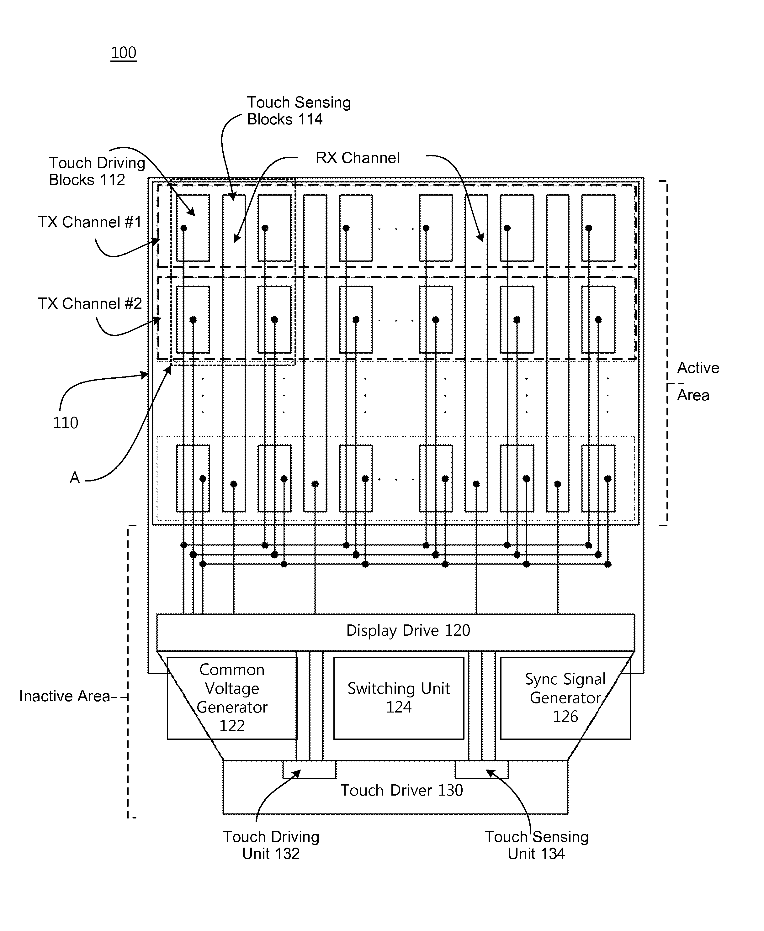
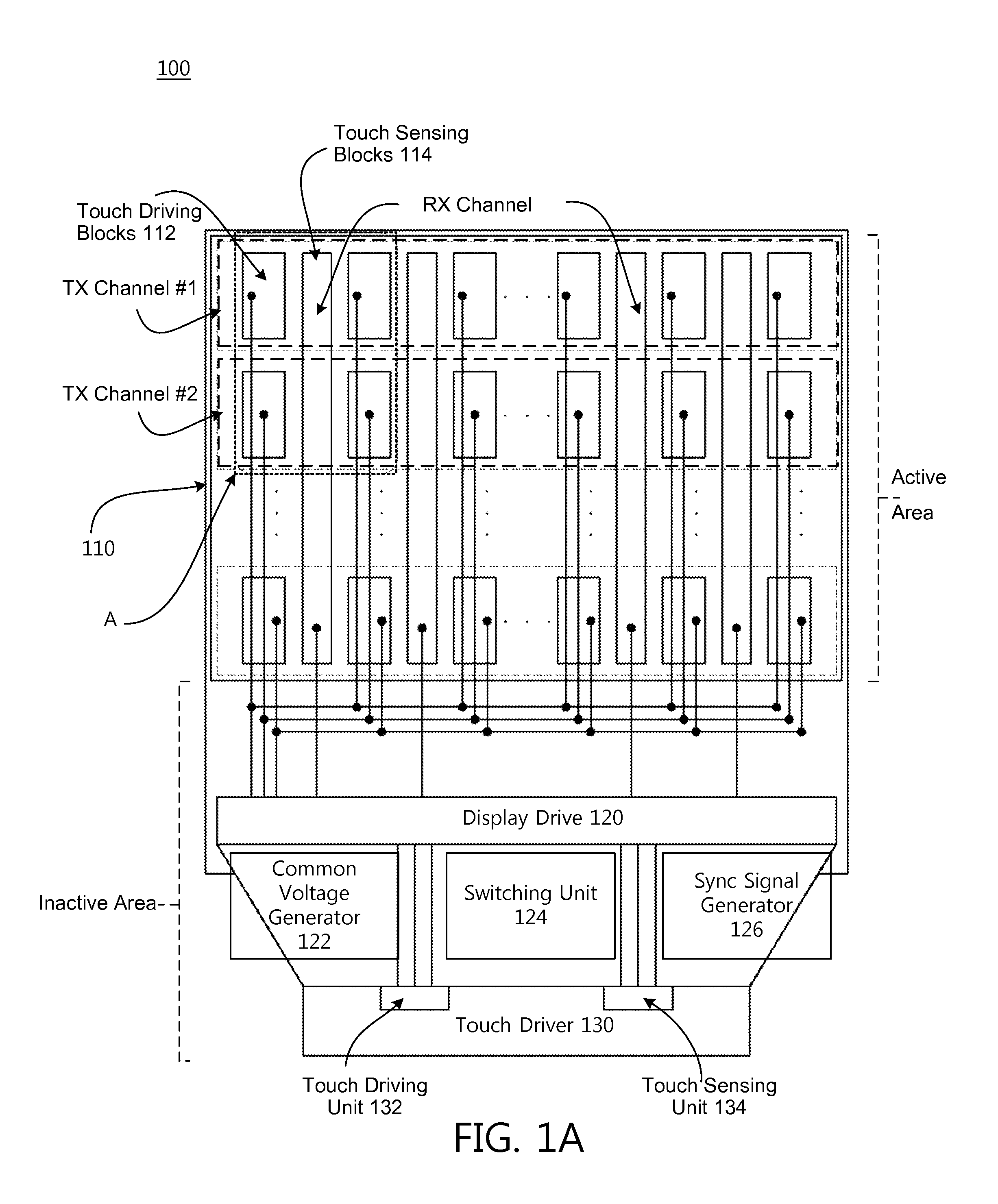
[0023]The following description includes embodiments described in the context of LCDs, in particular an In-Plane-Switching (IPS) mode LCD and / or a Fringe-Field-Switching (FFS) mode LCD, in which the touch driving blocks and touch sensing blocks (e.g., common electrodes) are formed on a lower substrate together with pixel electrodes. However, it should be appreciated that the features described in the present disclosure may be applied to organic light emitting diode (OLED) displays, electrophoretic displays, field emission displays and various other types of display devices.

[0024]Example embodiments may be described herein with reference to a Cartesian coordinate system in which the x-direction and the y-dire...


PUM


Abstract

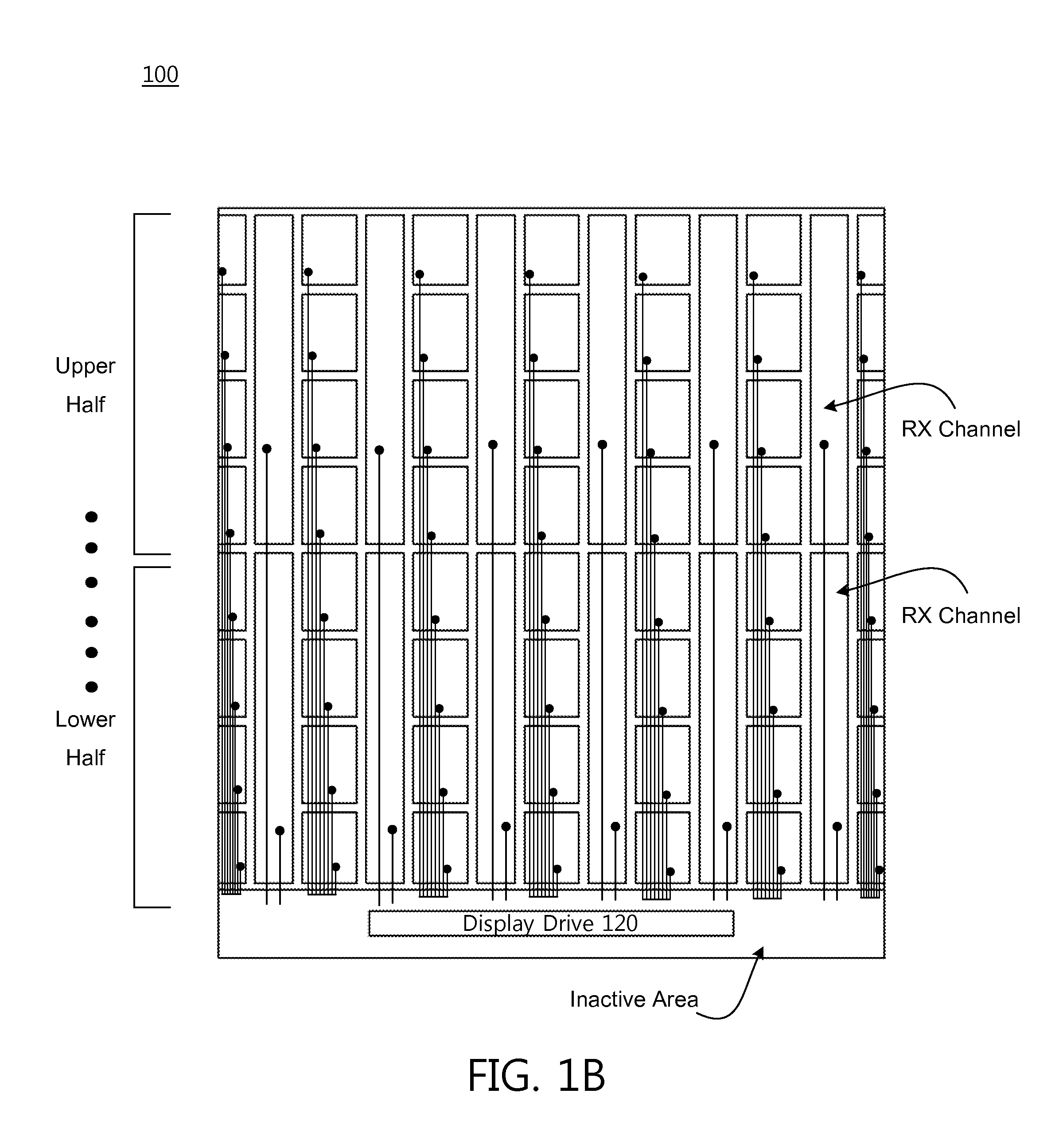
A touch sensor integrated display device includes a plurality of common electrode blocks serving as touch driving blocks and touch sensing blocks. Conductive lines connected to the touch driving blocks and touch sensing blocks are routed towards an inactive area of the display device by directly across the active area. The conductive lines are positioned within one or more organic dielectric layers formed under the common electrode blocks and pixel electrodes, but above the data lines of the display device.

Description

BACKGROUND OF THE INVENTION[0001]1. Field of the Invention[0002]The present disclosure generally relates to a display device, and more particularly to a display device configured for advanced mutual capacitance touch sensing and a method for manufacturing the same.[0003]2. Description of the Related Art[0004]Touch screens have been one of the most popular user input mechanism in a variety of electronic devices because of their ease and versatility of operation. Such a touch screen allows to identify the occurrence and position of a user's touches on the screen, enabling the electronic device to respond appropriately. Conventionally, touch screens may be flat panel displays such as liquid crystal displays (LCDs) or organic light emitting diode (OLED) displays overlaid with a touch panel.[0005]Conventionally, a grid of touch driving lines and touch sensing lines or a separate touch panel with the touch driving and sensing lines are overlaid across a display device. These touch drive a...

Claims


Application Information

Patent Timeline
IPC IPC(8): G06F3/041G06F3/044
CPCG06F3/0412G06F3/0416G06F3/044G06F3/04164G06F3/04166G06F3/0443G06F3/0446
Inventor YU, JAE SUNGHWANG, SANGSOO
Owner LG DISPLAY CO LTD
Learn More