
Organic layer deposition apparatus, method of manufacturing organic light emitting display device using the apparatus, and organic light emitting display device manufactured using the method

a technology deposition apparatuses, which is applied in the direction of chemical vapor deposition coatings, coatings, vacuum evaporation coatings, etc., can solve the problems of affecting the recent trend towards high-definition patterns, and affecting the quality of organic light-emitting display devices

Inactive Publication Date: 2016-04-21
SAMSUNG DISPLAY CO LTD
View PDF0 Cites 6 Cited by
  • Summary
  • Abstract
  • Description
  • Claims
  • Application Information

AI Technical Summary

Benefits of technology

The apparatus enables the production of high-definition organic light-emitting display devices on large substrates with improved manufacturing efficiency and reduced defects, addressing the limitations of traditional methods by allowing for precise and efficient deposition of organic layers.

Problems solved by technology

However, the deposition method using such an FMM presents difficulties in manufacturing larger organic light-emitting display devices using a large mother glass.
For example, when such a large mask is used, the mask may bend due to a gravitational pull, thereby distorting its pattern.
Such disadvantages are not conducive to the recent trend towards high-definition patterns.
Moreover, processes of aligning a substrate and an FMM to closely contact each other, performing deposition thereon, and separating the FMM from the substrate are time-consuming, resulting in a long manufacturing time and low production efficiency.

Method used


Image

  • Organic layer deposition apparatus, method of manufacturing organic light emitting display device using the apparatus, and organic light emitting display device manufactured using the method
  • Organic layer deposition apparatus, method of manufacturing organic light emitting display device using the apparatus, and organic light emitting display device manufactured using the method
  • Organic layer deposition apparatus, method of manufacturing organic light emitting display device using the apparatus, and organic light emitting display device manufactured using the method

Examples


Embodiment Construction

[0056]Reference will now be made in detail to the present embodiments of the present invention, examples of which are illustrated in the accompanying drawings, wherein like reference numerals refer to the like elements throughout. The embodiments are described below in order to explain aspects of the present invention by referring to the figures. Expressions such as “at least one of,” when preceding a list of elements, modify the entire list of elements and do not modify the individual elements of the list.

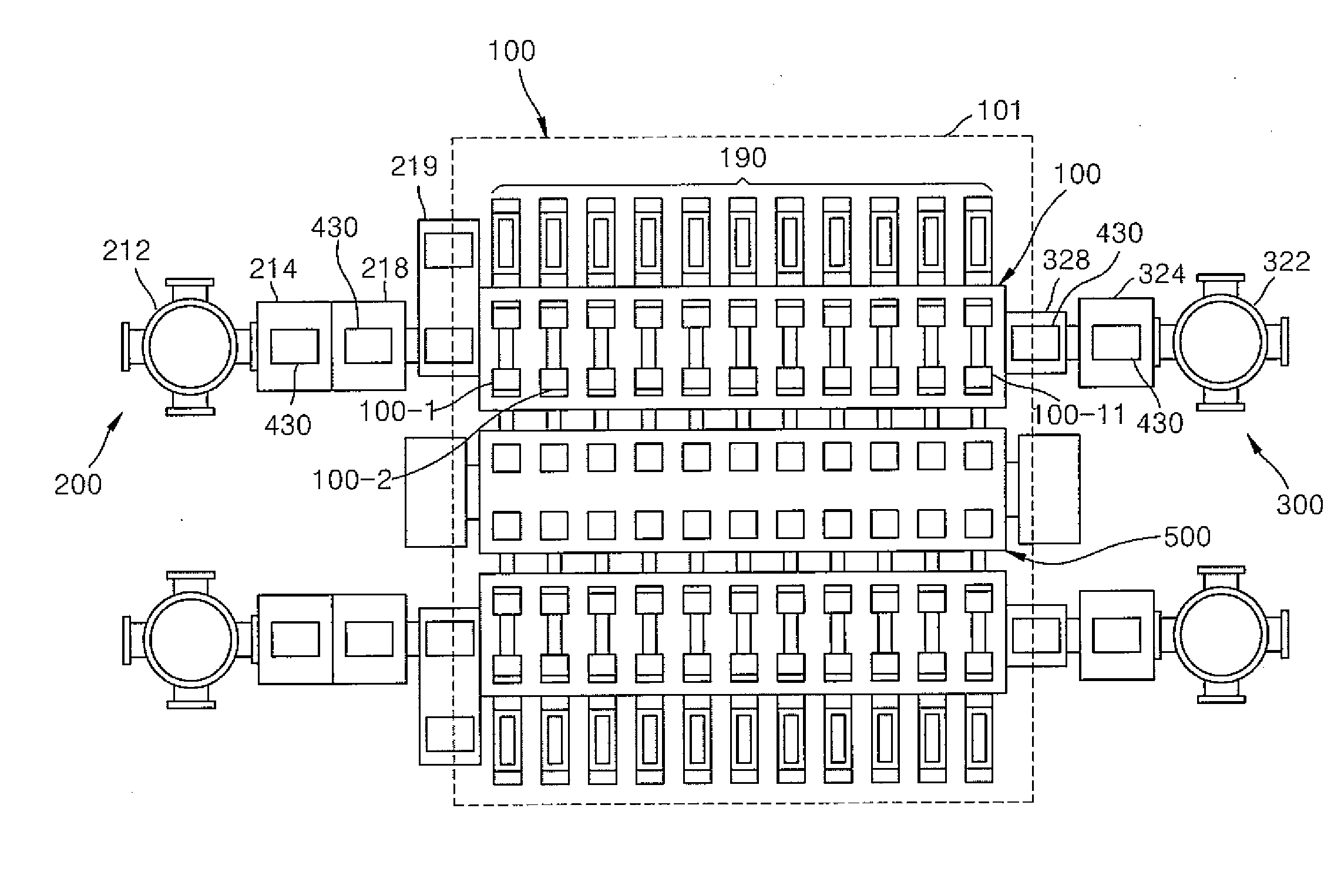
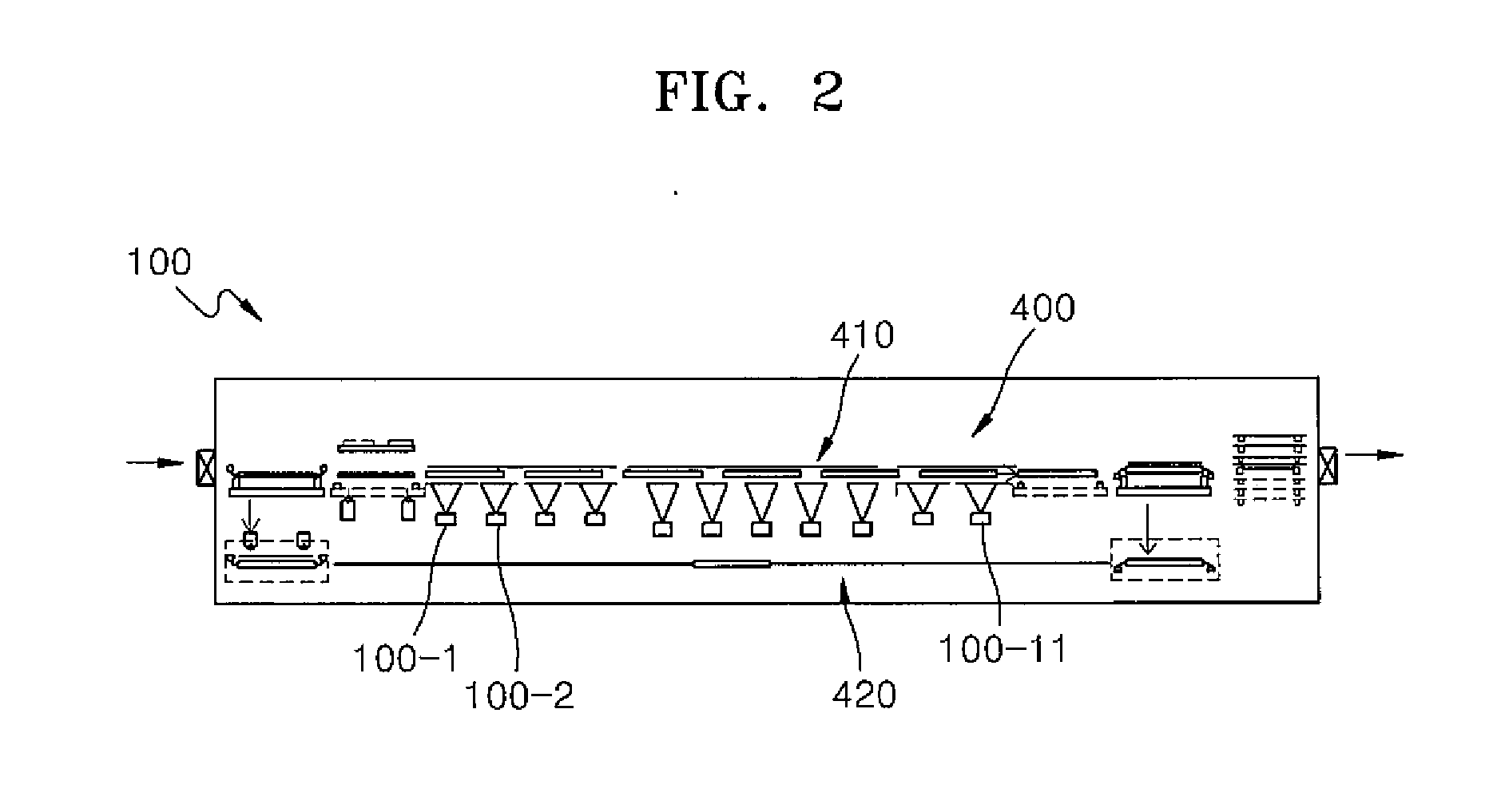
[0057]FIG. 1 is a schematic plan view illustrating a structure of an organic layer deposition apparatus 1 according to an embodiment of the present invention. FIG. 2 is a schematic side view of a deposition unit 100 of the organic layer deposition apparatus 1 of FIG. 1, according to an embodiment of the present invention.

[0058]Referring to FIGS. 1 and 2, the organic layer deposition apparatus 1 includes the deposition unit 100, a loading unit 200, an unloading unit 300, and a conv...


PUM


Abstract

An organic layer deposition apparatus, a method of manufacturing an organic light-emitting display device by using the same, and an organic light-emitting display device manufactured using the method, and in particular, an organic layer deposition apparatus that is suitable for use in the mass production of a large substrate and enables high-definition patterning, a method of manufacturing an organic light-emitting display device by using the same, and an organic light-emitting display device manufactured using the method.

Description

CROSS-REFERENCE TO RELATED PATENT APPLICATION[0001]This application is a divisional of U.S. patent application Ser. No. 13 / 791,899, filed on Mar. 8, 2013, which claims priority to and the benefit of Korean Patent Application No. 10-2012-0075142, filed on Jul. 10, 2012, in the Korean Intellectual Property Office, the disclosure of which is incorporated herein in its entirety by reference.BACKGROUND[0002]1. Field of the Invention[0003]The following description relates to an organic layer deposition apparatus, a method of manufacturing an organic light emitting display apparatus using the apparatus, and an organic light emitting display apparatus manufactured using the method, and more particularly, to an organic layer deposition apparatus that is suitable for use in mass production of a large substrate and enables high definition patterning, a method of manufacturing an organic light emitting display apparatus by using the apparatus, and an organic light emitting display apparatus man...

Claims


Application Information

Patent Timeline
Patent Type & Authority Applications(United States)
IPC IPC(8): H01L51/56C23C16/04C23C14/04C23C16/458H01L51/00C23C14/50H10K99/00
CPCH01L51/56H01L51/001H01L51/0011C23C16/042C23C14/042C23C16/458C23C14/50C23C14/568H10K71/166H10K71/441H10K71/20H01L21/67745H01L21/6776H10K71/00H10K50/30H10K71/10H10K71/13H10K71/164
Inventor HAN, KYU-SEOB
Owner SAMSUNG DISPLAY CO LTD
Features
  • Generate Ideas
  • Intellectual Property
  • Life Sciences
  • Materials
  • Tech Scout
  • Unparalleled Data Quality
  • Higher Quality Content
  • 60% Fewer Hallucinations
Learn More