Array substrate and method for fabricating the same, and display device and method for driving the same

Active Publication Date: 2016-04-28
SHANGHAI TIANMA MICRO ELECTRONICS CO LTD +1
View PDF33 Cites 10 Cited by
  • Summary
  • Abstract
  • Description
  • Claims
  • Application Information

AI Technical Summary

Benefits of technology

The patent describes an array substrate for a display device that includes a touch control signal driving line connected to a gate line for touch control detection and display scan synchronization. The technical effect of this design is that it eliminates the need to reduce the time of the display scan for each frame of picture, thereby avoiding undercharging of pixels and improving the performance of the display device, particularly for large-sized displays.

Problems solved by technology

However, in a conventional in-cell touch-control display device, a poor performance of a dark line or a bright line may be caused by an undercharge of pixels.
Particularly, such poor performance due to the undercharge becomes more apparent in large-size display devices.

Method used


Image

  • Array substrate and method for fabricating the same, and display device and method for driving the same
  • Array substrate and method for fabricating the same, and display device and method for driving the same
  • Array substrate and method for fabricating the same, and display device and method for driving the same

Examples


Embodiment Construction

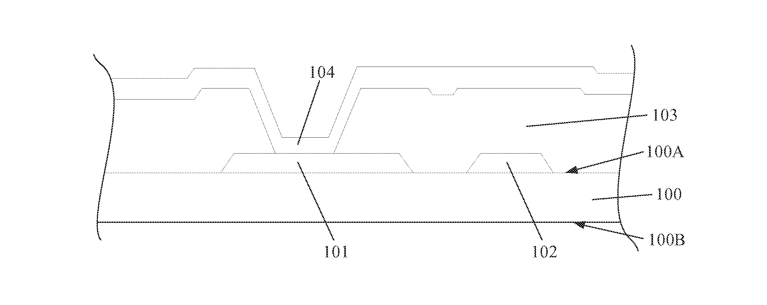
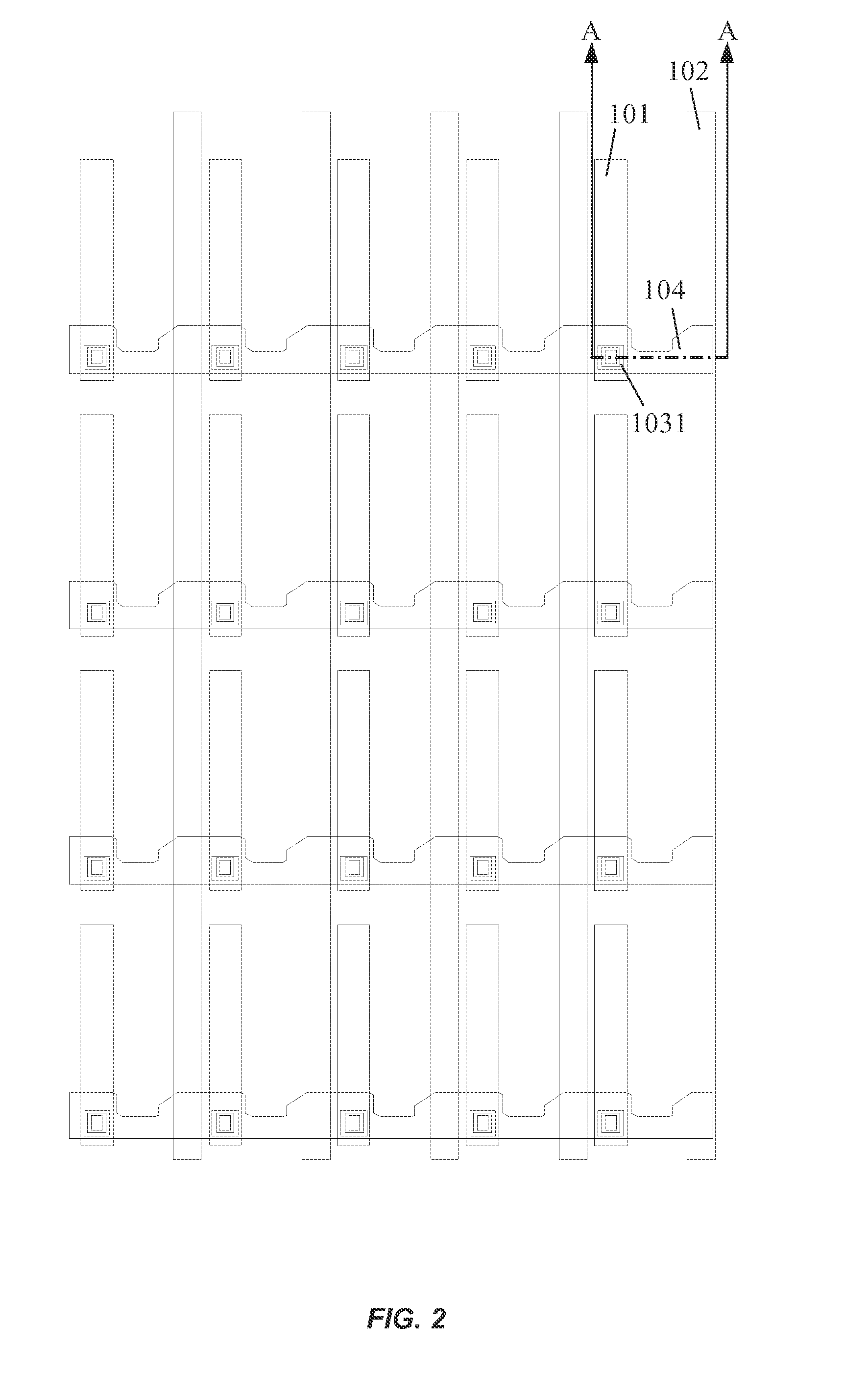
[0023]In order to prevent interference between the display signal and the touch control signal, a time-sharing scanning mode is adopted generally for the conventional in-cell touch-control display device. That is, for each frame of picture, the time for display scan is reduced, and the saved time is used for touch control scan. However, the reduction of the time for display scan for each frame of picture causes the undercharge of pixels, thereby resulting in a poor performance of a dark line or bright line in the displayed picture. Particularly, such poor performance due to the undercharge becomes more apparent for large-size display devices.

[0024]For this purpose, an array substrate is provided according to the disclosure. The array substrate includes a touch control signal driving line connected to a gate line, where a touch control detection is performed on the array substrate, and a display scan is performed on the array substrate synchronously. Thereby it is not necessary to re...


PUM


Abstract

An array substrate and a method for fabricating the array substrate, a display device and a method for driving the display device are provided. The array substrate includes: a substrate having a first surface and a second surface; a touch control signal driving line disposed on the first surface; an isolation layer disposed on the first surface and covering the touch control signal driving line; a via hole formed in the isolation layer; and a gate line disposed on the isolation layer and electrically connected to the touch control signal driving line through the via hole. The scanning time of the array substrate is not reduced due to a touch control detection, and the undercharge of pixels is thus avoided.

Description

CROSS-REFERENCES TO RELATED APPLICATIONS[0001]This application claims the benefit of priority to Chinese Patent Application No. 201410588216.4, filed with the Chinese Patent Office on Oct. 28, 2014 and entitled “ARRAY SUBSTRATE AND METHOD FOR FABRICATING THE SAME, AND DISPLAY DEVICE AND METHOD FOR DRIVING THE SAME,” the content of which is incorporated herein by reference in its entirety.TECHNICAL FIELD[0002]The disclosure relates to photoelectric technology, and more particular to an array substrate and a method for fabricating an array substrate, a display device and a method for driving a display device.BACKGROUND OF THE INVENTION[0003]Display technology plays an important role in the development of the current technology. Currently, display technologies mainly include liquid crystal display (LCD) technology, light emitting diode (LED) technology and organic light-emitting diode (OLED) technology.[0004]Display technology and touch control technology can be combined to form a disp...

Claims


Application Information

Patent Timeline
IPC IPC(8): G06F3/041H01L27/12
CPCG06F3/0416G06F2203/04103H01L27/1259G06F3/0412G06F3/044G09G3/20G02F1/13338G06F3/04164G06F3/04166G06F3/04184G06F3/0443G06F3/0446
Inventor ZHAO, JIAN
Owner SHANGHAI TIANMA MICRO ELECTRONICS CO LTD
Why Eureka
Try Eureka