Vertical and 3D memory devices and methods of manufacturing the same

a memory device and 3d memory technology, applied in the direction of semiconductor devices, basic electric elements, electrical equipment, etc., can solve the problems of ridge-like stacks bending or wiggle, complex patterning technologies, and nand architectures and other high density structures

Active Publication Date: 2016-05-19
MACRONIX INT CO LTD
View PDF0 Cites 133 Cited by
  • Summary
  • Abstract
  • Description
  • Claims
  • Application Information

AI Technical Summary

Problems solved by technology

The formation of conductive lines that include vertical columns between ridges in high aspect ratio trenches, such as those used in the 3DVG architecture, the vertical NAND architectures and other high density structures, can

Method used


Image

  • Vertical and 3D memory devices and methods of manufacturing the same
  • Vertical and 3D memory devices and methods of manufacturing the same
  • Vertical and 3D memory devices and methods of manufacturing the same

Examples


Embodiment Construction

[0052]A detailed description of embodiments of the present invention is provided with reference to the FIGS. 1-32.

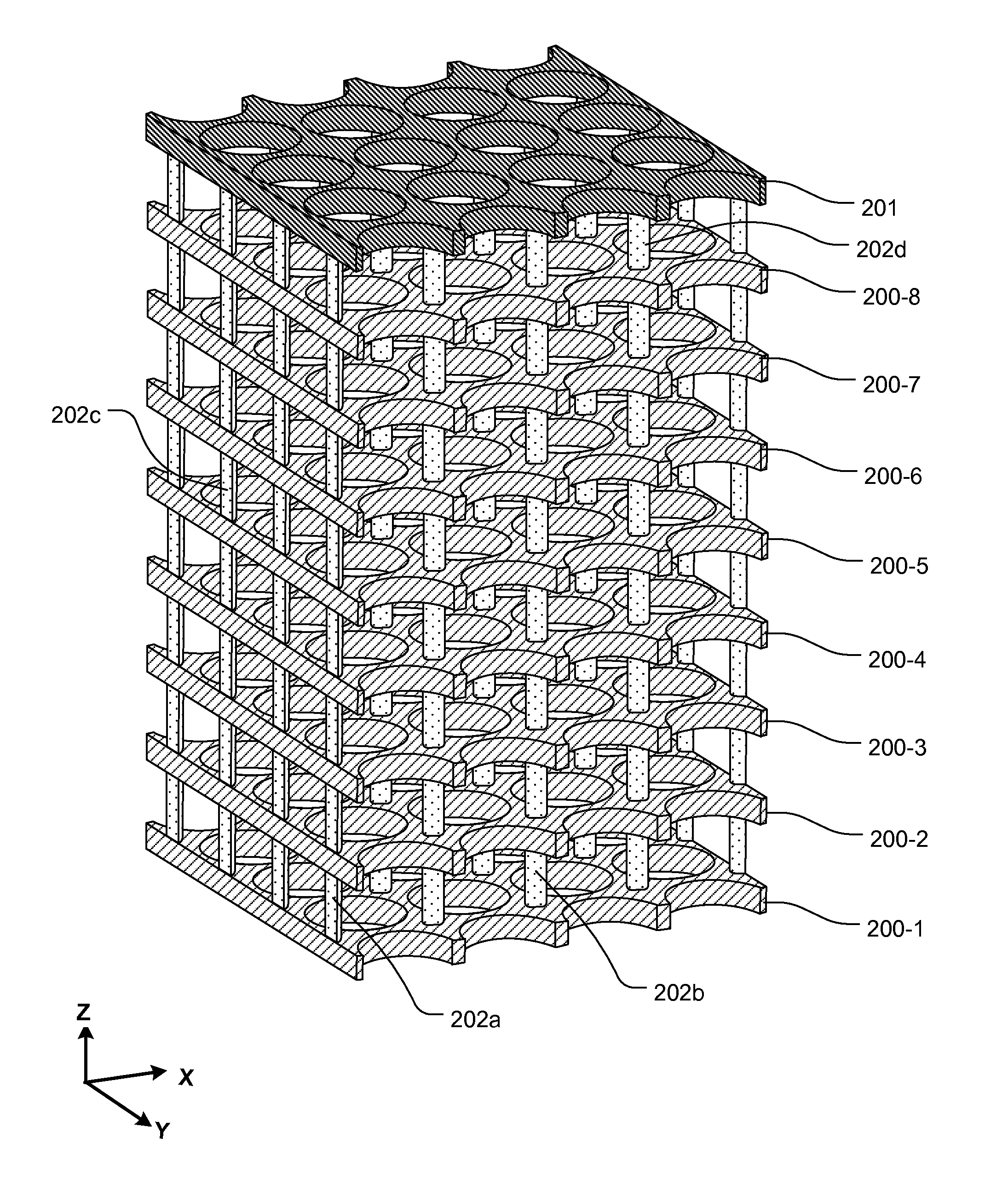
[0053]FIG. 1 is a perspective illustration of a prior art 3D vertical gate (3DVG) NAND-flash memory array structure as described in U.S. Pat. No. 8,503,213 having multiple layers of horizontal semiconductor strips configured as NAND string bit lines, and multiple patterned conductive lines crossing the strips that act as word lines, with vertical extensions between stacks of strips in the layers. In FIG. 1, insulating material is removed from the drawing to expose additional structure. For example, insulating layers are removed between the semiconductor strips, in the ridge-shaped stacks, and are removed between the ridge-shaped stacks of semiconductor strips.

[0054]The multilayer array is formed on an insulating layer, and includes patterned polysilicon layers providing a plurality of word lines 125-1, . . . , 125-N−1, 125-N conformal with a plurality of ridge-shaped sta...


PUM


Abstract

A memory device is described, which includes a block of memory cells comprising a plurality of stacks of horizontal active lines such as NAND string channel lines, with a plurality of vertical slices penetrated by, and surrounding, the horizontal active lines to provide a gate-all-around structure. A memory film is disposed between the horizontal active lines in the plurality of stacks and the vertical slices in the plurality of vertical slices. A 3D, horizontal channel, gate-all-around NAND flash memory is provided. A method for manufacturing a memory involves a buttress process. The buttress process enables horizontal channel, gate-all-around structures.

Description

BACKGROUND OF THE INVENTION[0001]1. Field of the Invention[0002]The present invention relates to high density integrated circuit devices. In particular, embodiments according to the present invention provide a method for manufacturing and a structure for a high density device.[0003]2. Description of Related Art[0004]As critical dimensions of devices in integrated circuits shrink to the limits of common memory cell technologies, designers have been developing techniques for stacking multiple planes of memory cells to achieve greater storage capacity, and to achieve lower costs per bit. For example, thin film transistor techniques are applied to charge trapping memory technologies in Lai, et al., “A Multi-Layer Stackable Thin-Film Transistor (TFT) NAND-Type Flash Memory,” IEEE Int'l Electron Devices Meeting, 11-13 Dec. 2006; and in Jung et al., “Three Dimensionally Stacked NAND Flash Memory Technology Using Stacking Single Crystal Si Layers on ILD and TANOS Structure for Beyond 30 nm ...

Claims


Application Information

Patent Timeline
IPC IPC(8): H01L27/115H01L21/28H01L29/423H01L29/51
CPCH01L27/11578H01L29/4234H01L21/28282H01L29/511H01L29/40114H01L29/40117H10B41/20H10B41/35H10B43/20H10B43/35
Inventor HONG, SHIH-PING
Owner MACRONIX INT CO LTD
Why Eureka
Try Eureka