Memory devices and methods of manufacturing the same

a memory device and manufacturing method technology, applied in the field of semiconductor devices, can solve the problems of increasing the cost of these devices, limiting the extent to which the integration densities of 2d memory devices are increased, and the cost of these apparatuses will only increas

Inactive Publication Date: 2016-05-26
SAMSUNG ELECTRONICS CO LTD
View PDF7 Cites 47 Cited by
  • Summary
  • Abstract
  • Description
  • Claims
  • Application Information

AI Technical Summary

Problems solved by technology

However, apparatuses for forming fine patterns are very expensive to begin with and the cost of these apparatuses will only increase along with the fineness of the patt

Method used


Image

  • Memory devices and methods of manufacturing the same
  • Memory devices and methods of manufacturing the same
  • Memory devices and methods of manufacturing the same

Examples


Embodiment Construction

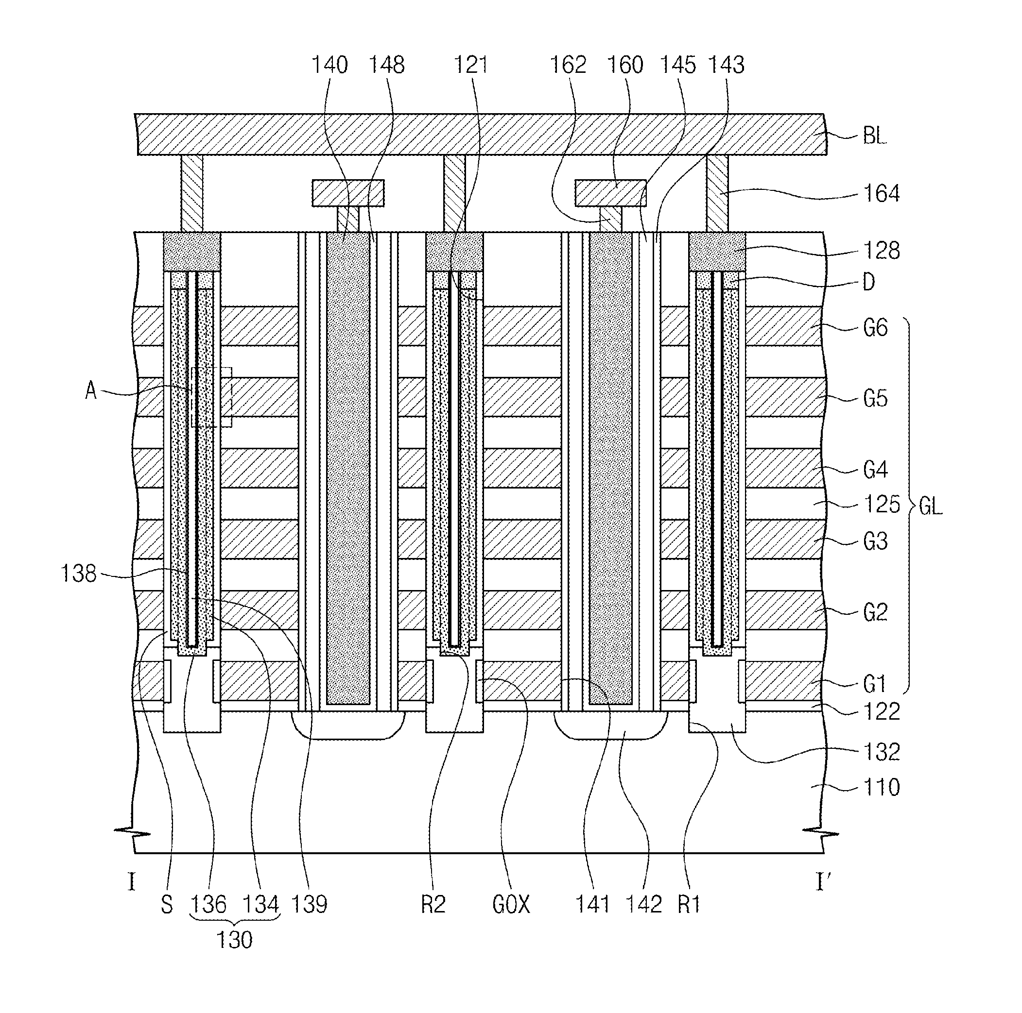
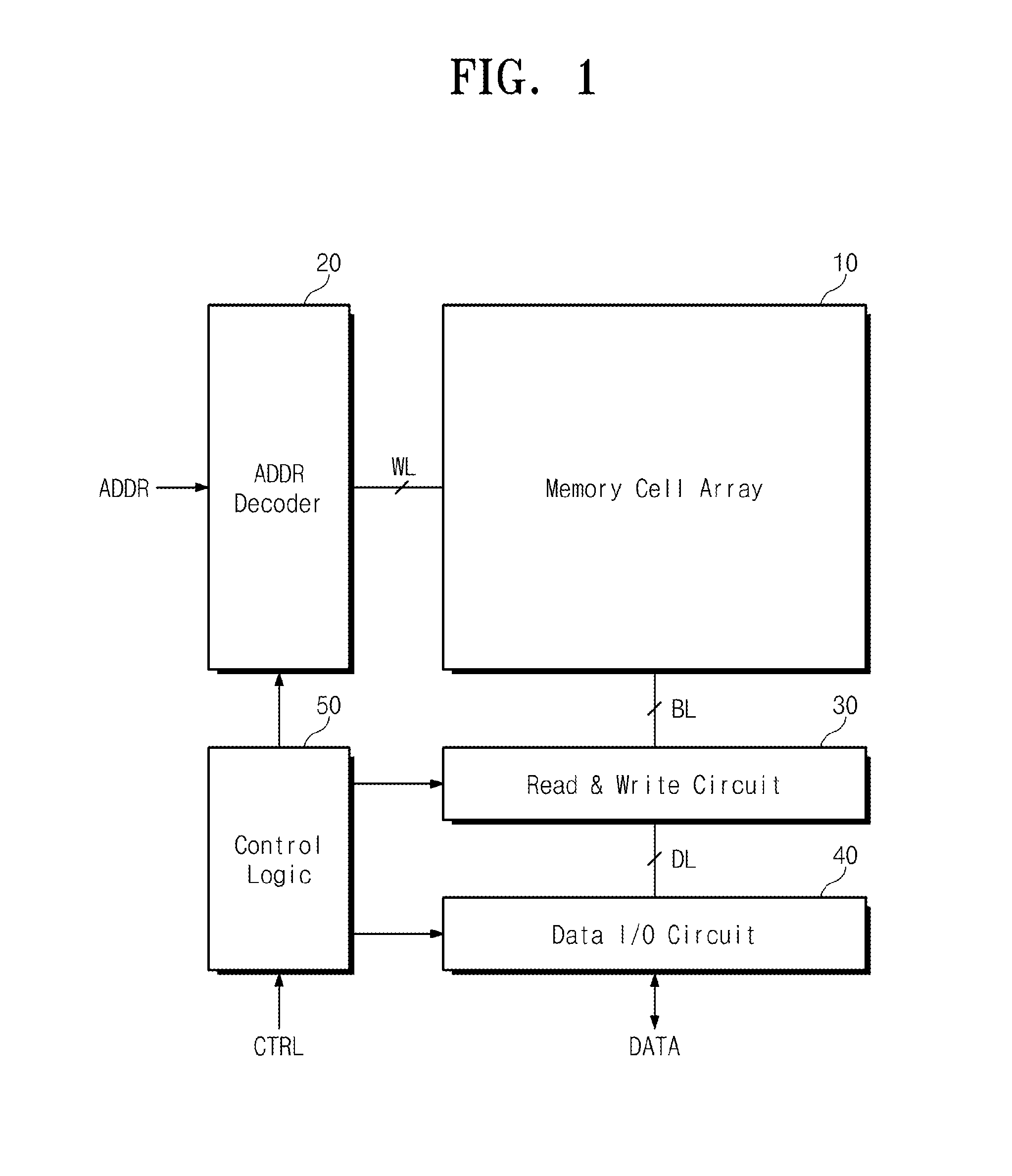
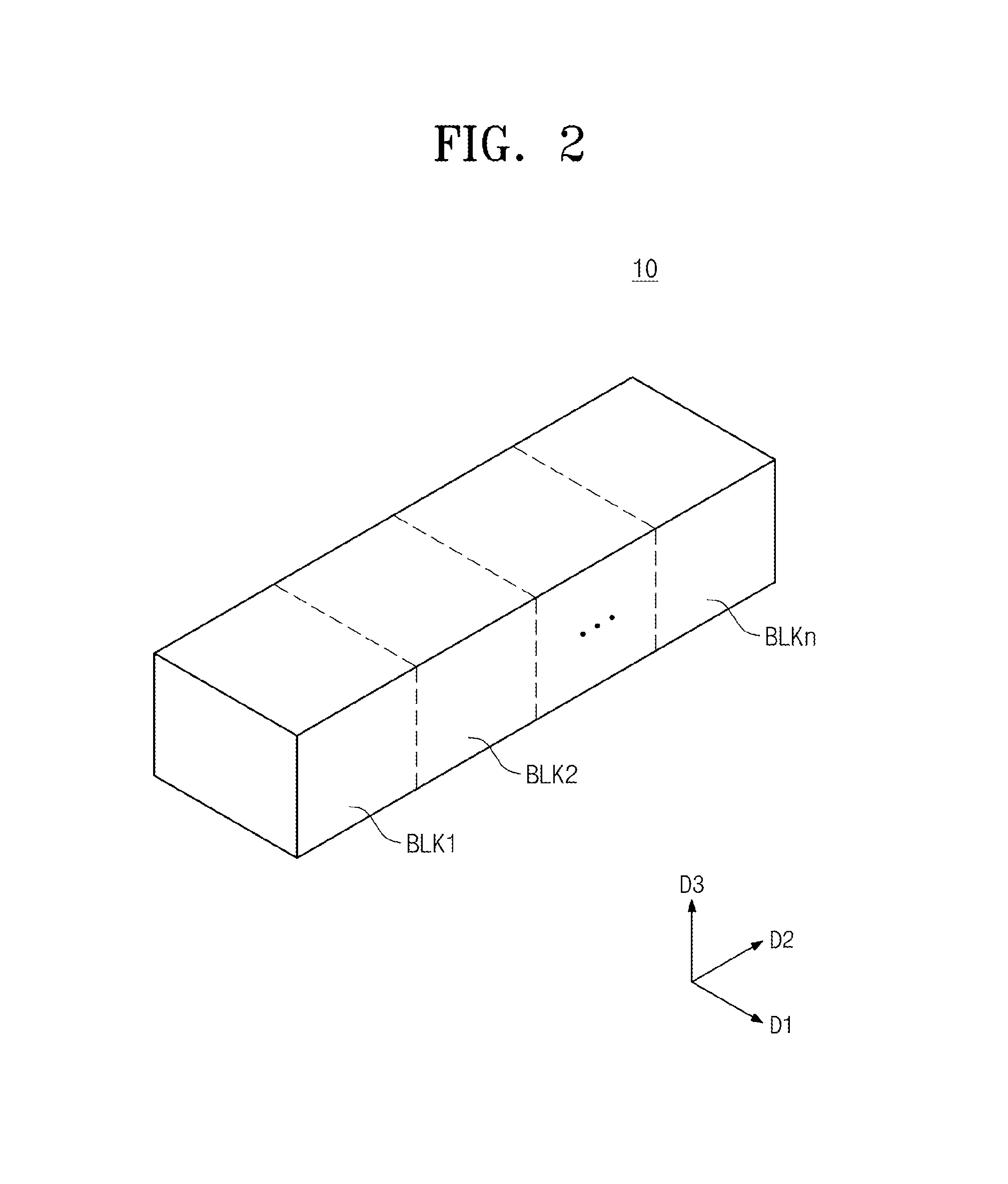
[0026]The inventive concepts will now be described more fully hereinafter with reference to the accompanying drawings, in which exemplary embodiments of the inventive concepts are shown. The advantages and features of the inventive concepts and methods of achieving them will be apparent from the following exemplary embodiments that will be described in more detail with reference to the accompanying drawings. It should be noted, however, that the inventive concepts are not limited to the following exemplary embodiments, and may be implemented in various forms. Accordingly, the exemplary embodiments are provided only to disclose the inventive concepts and let those skilled in the art know the category of the inventive concepts. In the drawings, embodiments of the inventive concepts are not limited to the specific examples provided herein and are exaggerated for clarity.

[0027]The terminology used herein is for the purpose of describing particular embodiments only and is not intended to...


PUM


Abstract

A memory device includes a stack including gate electrodes vertically stacked on a substrate and having a vertical hole, an active pillar disposed in the vertical hole and providing a vertical channel, a charge storage section interposed between the active pillar and the gate electrodes, a blocking dielectric interposed between the charge storage section and the gate electrodes, a tunnel dielectric interposed between the charge storage section and the active pillar, insulation filling an inner hole of the active pillar, and a fixed charge layer interposed between the filling insulation and the active pillar. Measures are taken to address phenomena in which current would otherwise be adversely affected near an interface between the vertical channel and the filling insulation.

Description

PRIORITY STATEMENT[0001]This U.S. non-provisional patent application claims priority under 35 U.S.C. §119 to Korean Patent Application No. 10-2014-0162643, filed on Nov. 20, 2014, in the Korean Intellectual Property Office, the disclosure of which is hereby incorporated by reference in its entirety.BACKGROUND[0002]The inventive concepts relate to semiconductor devices and methods of manufacturing the same. More particularly, the inventive concepts relate to three dimensional (3D) non-volatile memory devices and methods of manufacturing the same.[0003]The integration density of semiconductor memory devices may be proportional to the cost of the semiconductor memory devices. A conventional two-dimensional (2D) memory device includes a planar array of unit memory cells formed of fine patterns of certain elements and features. The integration density of such a conventional two-dimensional (2D) memory device mainly corresponds to the area occupied by a unit memory cell of the device. Thu...

Claims


Application Information

Patent Timeline
IPC IPC(8): H01L27/115
CPCH01L27/11582H01L27/11568H01L29/4234H01L29/42364H10B43/20H10B43/10H10B43/27H10B41/30
Inventor SEO, JUN-HOKANG, DAEWOONGBANG, HYOJELEE, CHANGSUBHUR, SUNGHOI
Owner SAMSUNG ELECTRONICS CO LTD
Why Eureka
Try Eureka