Supercharge Your Innovation With Domain-Expert AI Agents!

Zig-zag trench structure to prevent aspect ratio trapping defect escape

a technology of trench structure and aspect ratio, applied in the field of trench structure, can solve the problems of abrupt changes in electrical and/or optical properties, difficult integration of semiconductor materials on silicon, and material impact on the performance of devices fabricated using dissimilar semiconductor materials

Active Publication Date: 2016-06-23
TAIWAN SEMICON MFG CO LTD
View PDF5 Cites 0 Cited by
  • Summary
  • Abstract
  • Description
  • Claims
  • Application Information

AI Technical Summary

Benefits of technology

The present invention is about a semiconductor structure and a method of making it. The semiconductor structure includes a trench-defining layer, an epitaxial layer, and a set of defect-blocking members. The epitaxial layer is formed by epitaxial growth, and the trench-defining layer includes a trench surface that defines an elongated trench interior space. Each defect-blocking member of the set of defect-blocking members extends from the trench surface into the trench interior space. The epitaxial layer is located in the portions of the trench interior space not occupied by the set of defect-blocking members. The semiconductor structure can be used in a field-effect transistor (FET) device that includes a FET components set including a first gate and a first contact. The FET components set is located at least partially on top of a top surface of the epitaxial layer. The technical effects of this invention are that it provides a semiconductor structure and a method of making it that can prevent defects during epitaxial growth and improve the performance and reliability of semiconductor devices.

Problems solved by technology

III-V semiconductors have larger lattice constants than silicon, so integrating them on silicon is challenging.
The performance of devices fabricated using dissimilar semiconductor materials can be materially affected by defects that cause abrupt changes in electrical and / or optical properties.
Co-integration of III-V with silicon deals with a known challenge due to the high lattice mismatch of some III-V semiconductor materials and silicon (and germanium (Ge) and silicon-germanium (SiGe)).

Method used


Image

  • Zig-zag trench structure to prevent aspect ratio trapping defect escape
  • Zig-zag trench structure to prevent aspect ratio trapping defect escape
  • Zig-zag trench structure to prevent aspect ratio trapping defect escape

Examples


Embodiment Construction

[0026]Some embodiments of the present invention are directed to techniques for addressing defect issues in the manufacture of devices employing semiconductor materials having dissimilar properties, such as dissimilar lattice constants.

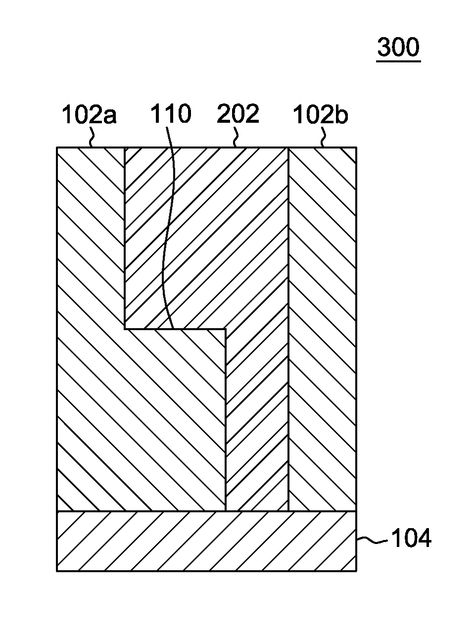
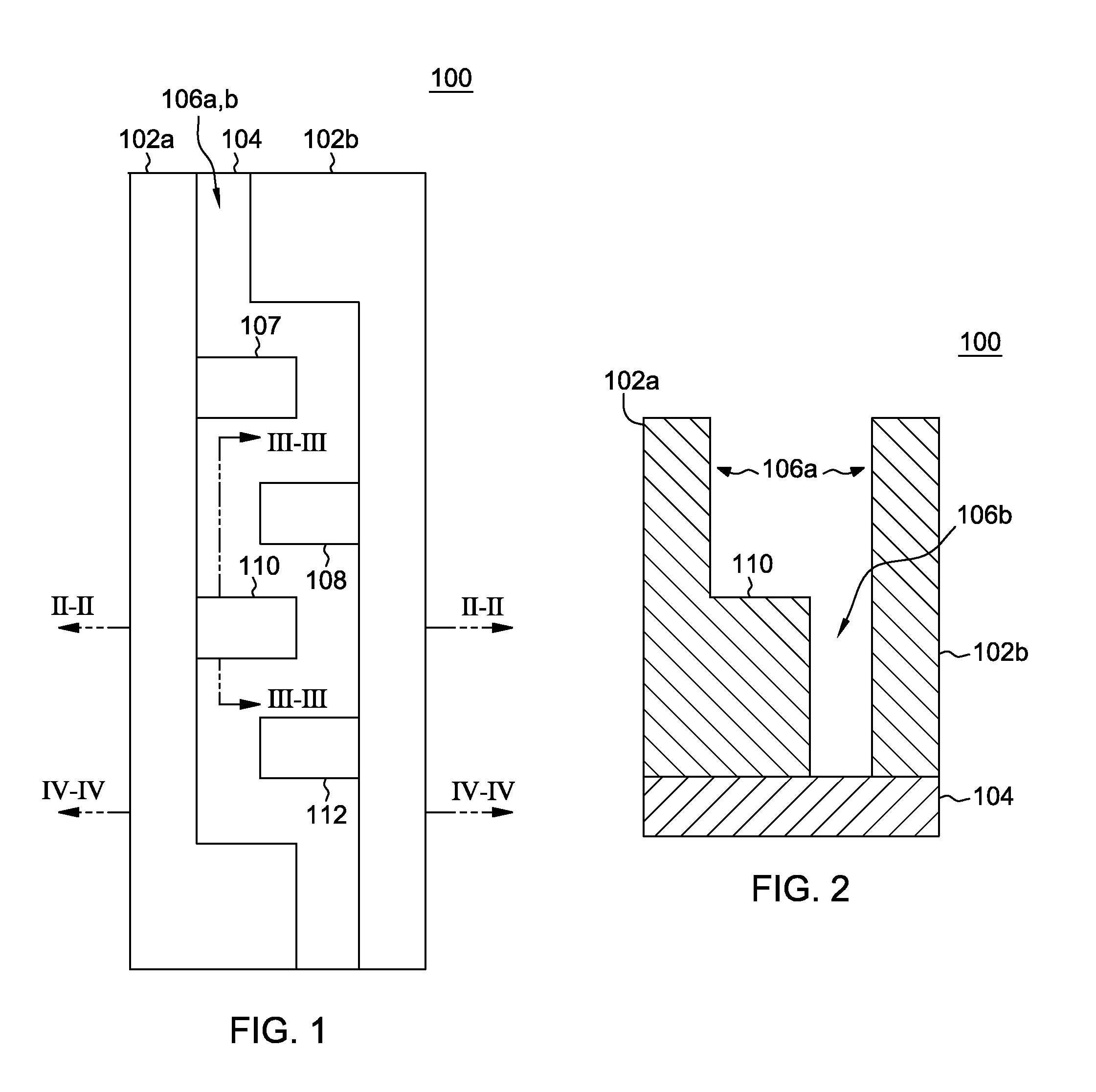
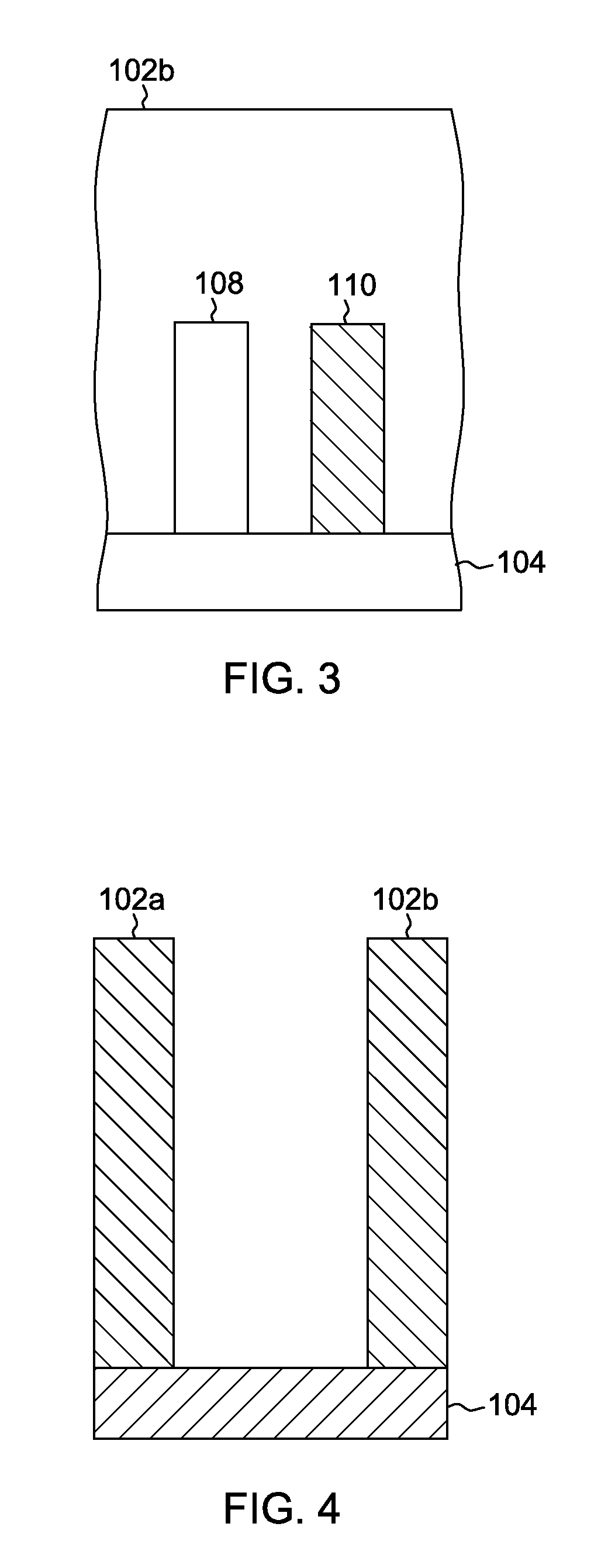
[0027]Some embodiments of the present invention recognize the following facts, potential problems and / or potential areas for improvement with respect to the current state of the art: the use of parallel trenches in ART style FETs leads to the problem of defects parallel to the direction of elongation of the trench “escaping.” More specifically, the recognized risk is that the semiconductor material used to fill the trench can, during its epitaxial growth inside the interior space of the trench, develop defects that propagate in a direction that is parallel, or at least generally parallel, to the direction of elongation of the trench. While the side walls that help define the trench will arrest defect propagation in a direction transverse, or at least g...


PUM


Abstract

A semiconductor structure including: trench-defining layer; an epitaxial layer; and a set of defect-blocking member(s). The trench-defining layer includes a trench surface which defines an elongated interior space called the “trench.” The epitaxial layer is grown epitaxially in the interior space of the trench. Each defect blocking member of the set of defect blocking members: (i) extends from a portion of trench surface into the interior space of the trench; and (ii) is located below a top surface of the epitaxial layer. The defect blocking member(s) are designed to arrest the propagation of generally-longitudinal defects in the epitaxial layer, as it is grown, where the generally-longitudinal defects are defects that propagate at least generally in the elongation direction of the trench.

Description

BACKGROUND OF THE INVENTION[0001]The present invention relates generally to the field of field-effect transistors (FETs, NFETs, PFETs), and more particularly to trench structures, for FETs, with relatively large lattice mismatch in their constituent materials.[0002]III-V semiconductors have larger lattice constants than silicon, so integrating them on silicon is challenging. Methods for integrating III-V semiconductors on silicon have included blanket III-V growth and aspect ratio trapping (ART). Many semiconductor materials, such as silicon (Si) have, at the atomic level, a lattice structure. When two different semiconductor materials are intermingled, or placed in close proximity, it is generally better if the lattice constants of the two semiconductor materials are compatible, as such compatibility is understood by those of skill in the art. Aspect ratio trapping is an effective technique to trap threading dislocations, thereby reducing the dislocation density of lattice mismatch...

Claims


Application Information

Patent Timeline
IPC IPC(8): H01L29/06H01L29/78H01L21/304H01L29/66H01L21/306H01L21/3065
CPCH01L29/0642H01L21/30625H01L29/78H01L21/3043H01L29/66477H01L21/3065H01L21/02381H01L21/02546H01L21/02647H01L29/66795H01L29/785H01L21/02639H01L29/66431H01L29/7786H01L29/66462H01L21/02458H01L21/02549H01L21/02636H01L21/7605H01L21/76248H01L21/76294
Inventor HOLT, JUDSON R.MOCHIZUKI, SHOGOREZNICEK, ALEXANDERSMITH, MELISSA A.
Owner TAIWAN SEMICON MFG CO LTD
Features
  • R&D
  • Intellectual Property
  • Life Sciences
  • Materials
  • Tech Scout
  • Unparalleled Data Quality
  • Higher Quality Content
  • 60% Fewer Hallucinations
Learn More