

Touch Sensor Integrated Type Display Device
- Summary
- Abstract
- Description
- Claims
- Application Information
AI Technical Summary
Benefits of technology
Problems solved by technology
Method used
Image

Examples
first embodiment
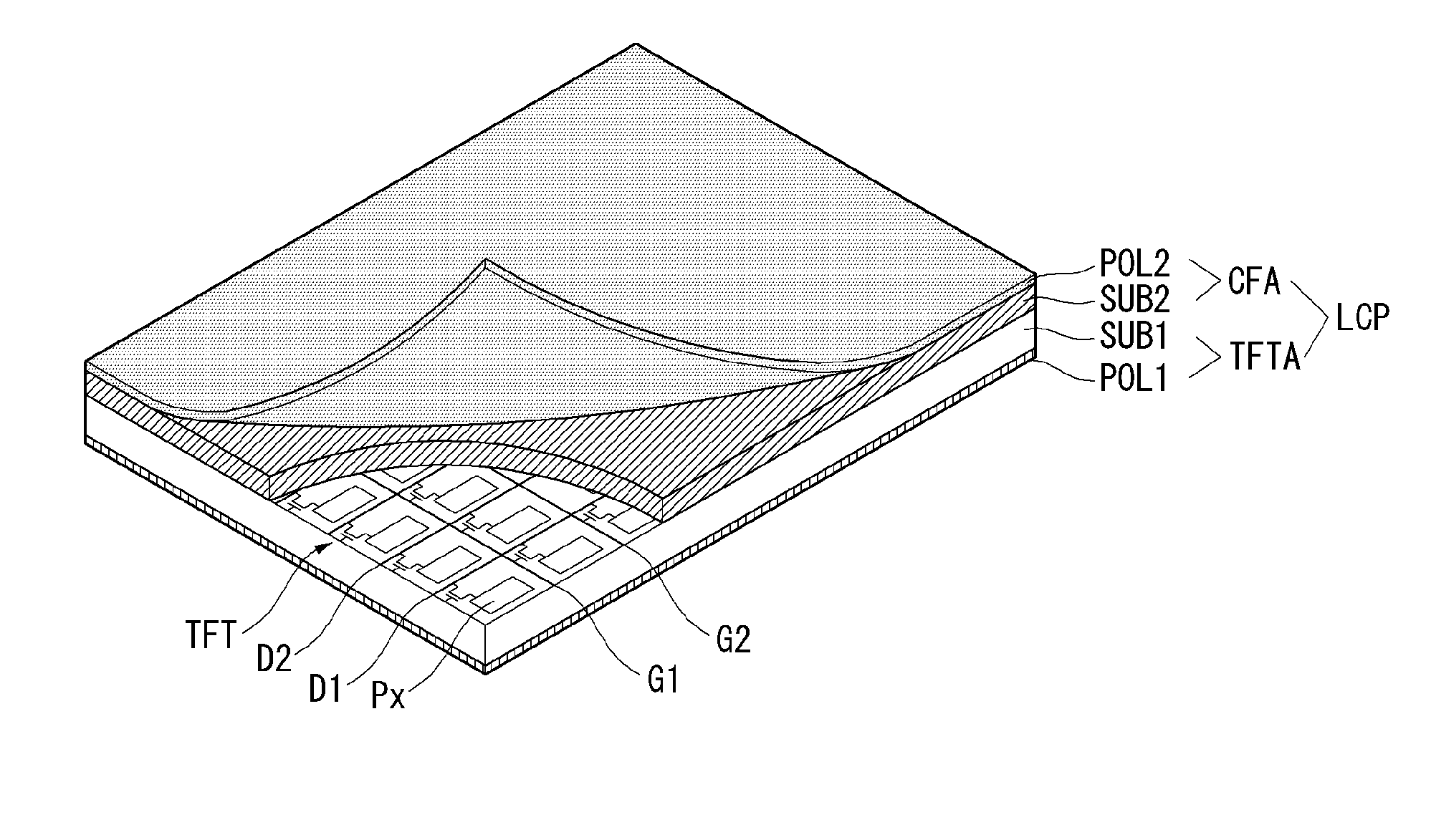
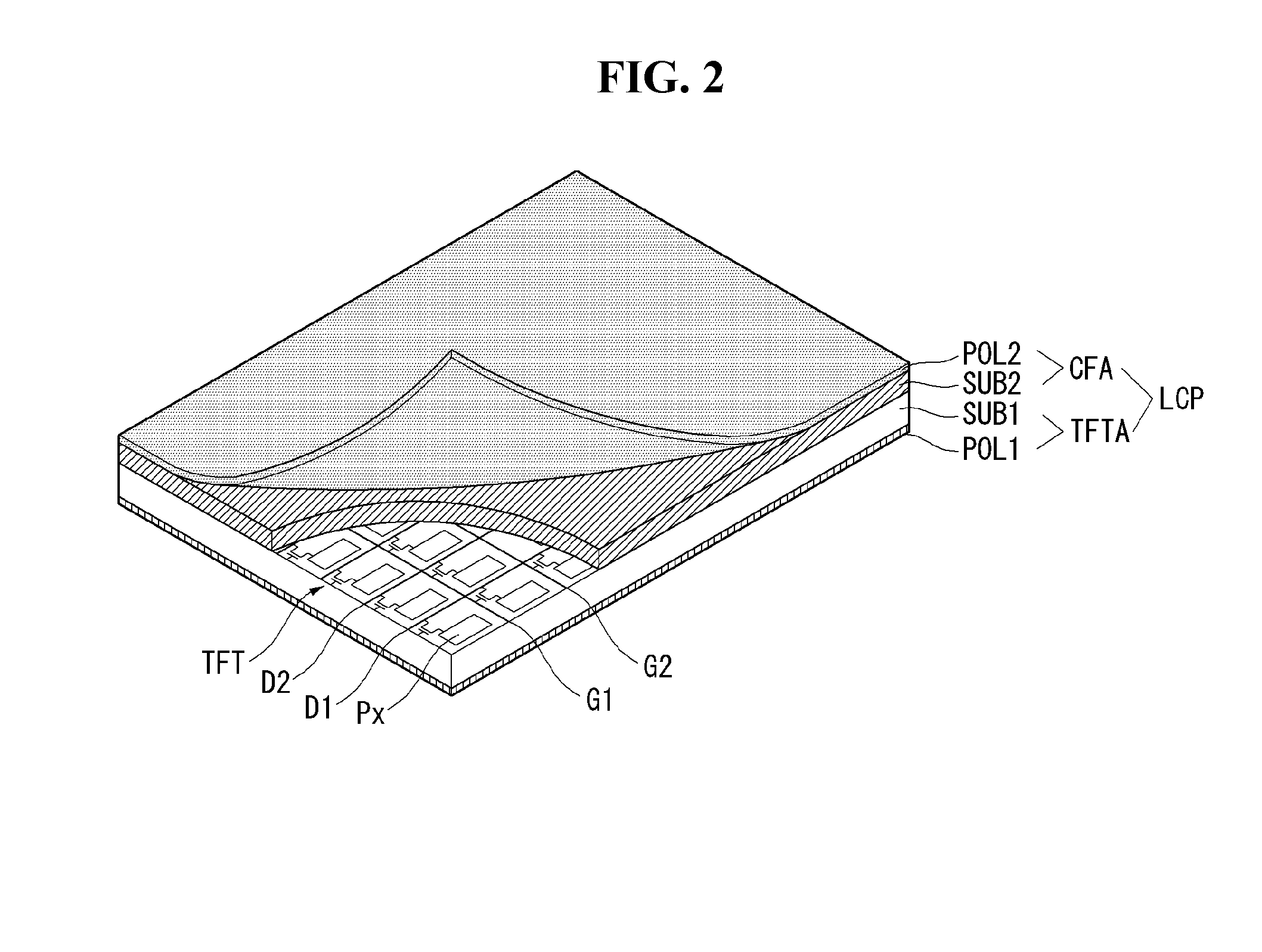
[0080]FIG. 2 is a partial exploded perspective view illustrating a touch sensor integrated type display device according to an embodiment of the present invention, and FIG. 3 is a planar view illustrating a relationship between touch / common electrodes and routing wires in a touch sensor integrated type display device according to the invention.
[0081]Referring to FIG. 2, the touch sensor integrated type display device includes a liquid crystal display panel LCP having a thin film transistor (TFT) array TFTA and a color filter array CFA that are facing each other, with a liquid crystal layer (not shown) interposed therebetween.
[0082]The TFT array TFTA includes a plurality of gate lines G1 and G2 (two gate lines G1 and G2 are shown, however the TFT array TFTA may include additional gate lines not shown) which may be arranged in parallel in a first direction (e.g., x-axis direction) on a first substrate SUB1, a plurality of data lines D1 and D2 (two data lines D1 and D2 are shown, howev...
second embodiment
[0118]Hereinafter, a touch sensor integrated type display device according to the invention will be described with reference to FIG. 10.
[0119]FIG. 10 is a planar view illustrating a relationship between touch / common electrodes and routing wires in a touch sensor integrated type display device according to the second embodiment of the invention.
[0120]Referring to FIG. 10, the touch sensor integrated display device according to the second embodiment of the invention includes an active area AA and a bezel area BA outside the active area AA. The active area AA is an area in which touch / common electrodes are arranged and data are displayed. The bezel area BA is an area in which various wires including routing wires extended from the active area AA for driving and sensing touch / common electrodes and display / touch controller ICs for driving source drivers and gate drivers may be disposed.
[0121]The active area AA may include a plurality of touch / common electrodes Tx11 to Tx19, Tx21 to Tx29,...
third embodiment
[0129]Hereinafter, a touch sensor integrated type display device according to the invention will be described with reference to FIG. 11.
[0130]FIG. 11 is a planar view illustrating a relationship between touch / common electrodes and routing wires in a touch sensor integrated type display device according to the third embodiment of the invention.
[0131]Referring to FIG. 11, the touch sensor integrated display device according to the third embodiment of the invention includes an active area AA and a bezel area BA outside the active area AA. The active area AA is an area in which touch / common electrodes Tx11 to Tx19, Tx21 to Tx29, Tx31 to Tx39, Tx41 to Tx49, Tx51 to Tx59, Tx61 to Tx69, Tx71 to Tx79, Tx81 to Tx89 and routing wires TW11 to TW19, TW21 to TW29, TW31 to TW39, TW41 to TW49, TW51 to TW59, TW61 to TW69, TW71 to TW79, TW81 to TW89 are arranged and data are displayed. The bezel area BA is an area in which various wires including routing wires extended from the active area AA for dr...
PUM
 Abstract
Description
Claims
Application Information