Display device and method of applying the same

a technology of display device and display position, applied in the field of display device and application method, can solve the problems of inability to accurately or sensing position, inability to adjust the position, so as to reduce the effect of capacitive coupling on touch sensing of the tp and enhance the touch sensitivity of the tp

Inactive Publication Date: 2010-12-16
AU OPTRONICS CORP
View PDF6 Cites 38 Cited by
  • Summary
  • Abstract
  • Description
  • Claims
  • Application Information

AI Technical Summary

Benefits of technology

[0010]One objects of the present invention is to provide a display device and method of applying the same. The display device is equipped with an additional shielding layer, which is interposed between the transparent conductive layer of the touch panel (TP) and the common electrode layer of the liquid crystal display panel (LCD panel). By controlling a first control signal and a second control signal, the effect of capacitive coupling on touch sensing of the TP can be reduced so that the touch sensitivity of the TP can be enhanced.

Problems solved by technology

But, because capacitive sensing circuits are easy to be affected by some noise produced by TFT-LCDs per se, surrounding environments, etc. to be distorted, resulting in incorrect response.
In this way, the sensitivity will worsen when the finger 5 touches the embedded touch panel 2, which makes it more difficult in sensing correctly or sensing positions.

Method used


Image

  • Display device and method of applying the same
  • Display device and method of applying the same
  • Display device and method of applying the same

Examples


Embodiment Construction

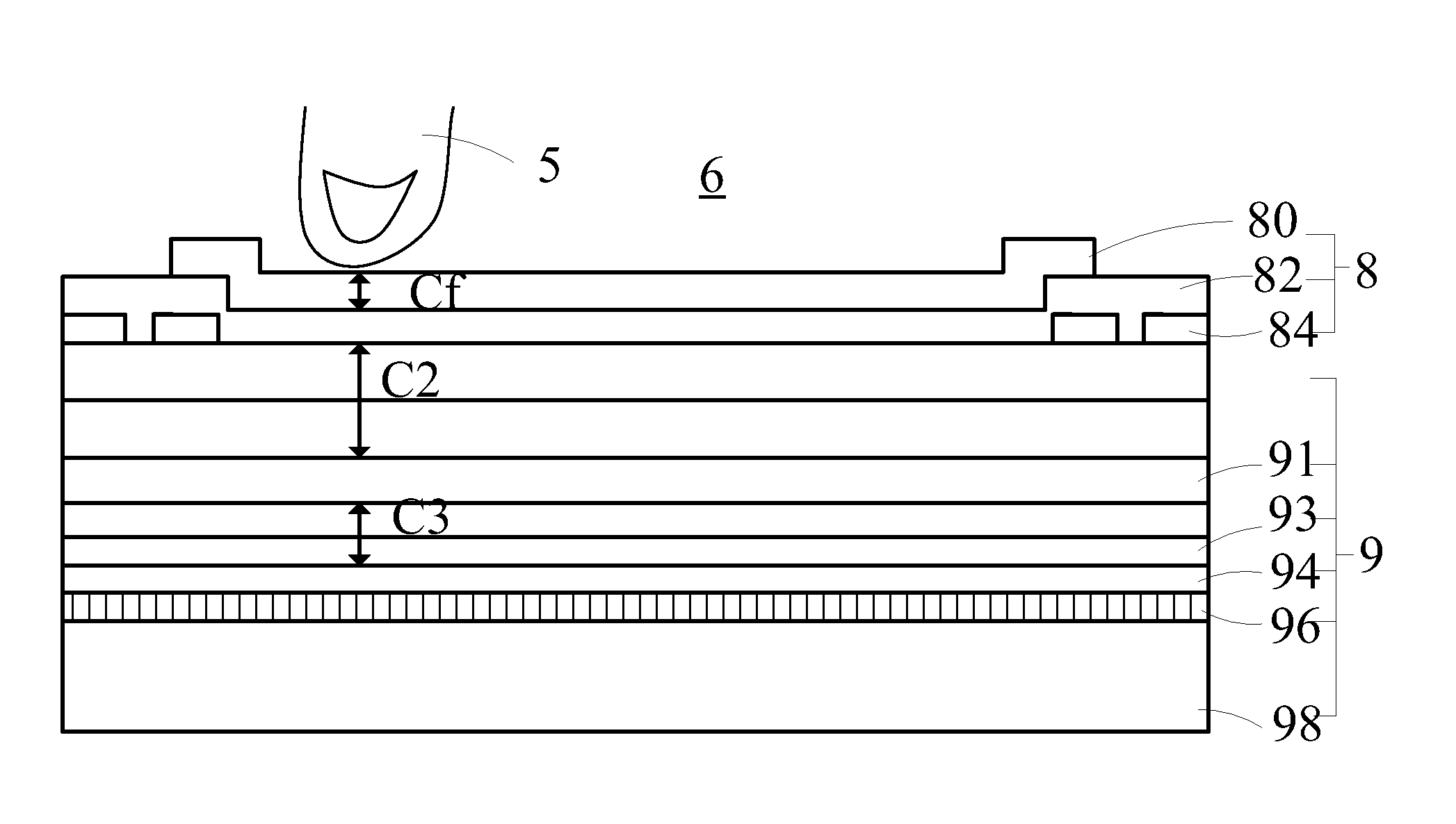
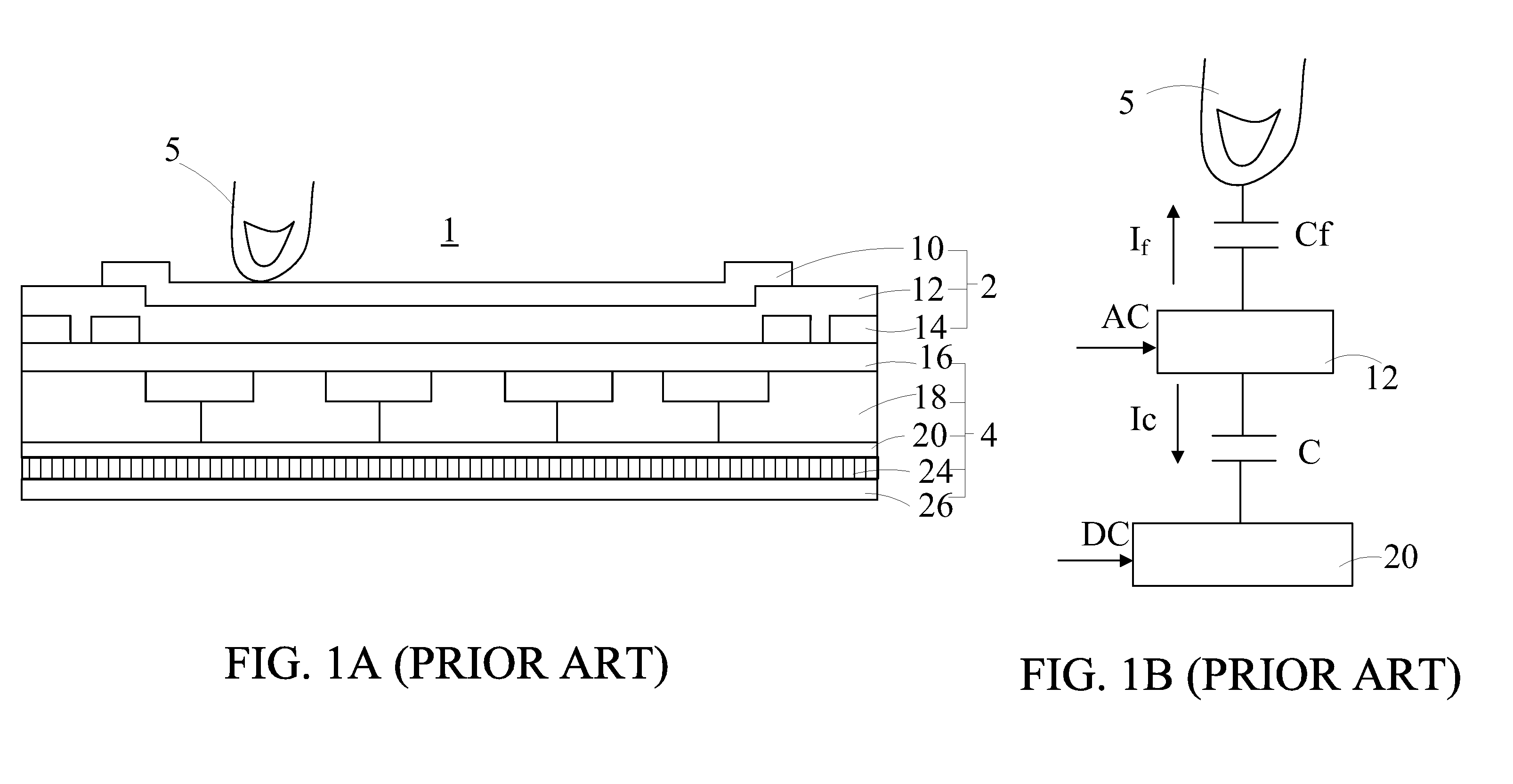
[0031]Please refer to FIGS. 2A and 2B, first. Both of the figures show a display device 6 of a first preferred embodiment of the present invention. The display device 6 mainly comprises a touch panel (TP) 8, a LCD panel 9, and at least one shielding layer 91. In the present embodiment, the TP 8, which can be either a surface capacitive touch panel, a projected capacitive touch panel, or other touch panels with similar technology, is embedded (e.g., film formation) on the upper surface of the LCD panel 9. The TP 8 comprises a polarized light contact layer 80 situated at the outermost layer position (e.g., a polarizer film (PF), which can act as a hard coater (HC) layer as well), which allows a part of the human body such as the finger 5 to touch directly, a transparent conductive layer 82 (e.g., ITO, which is situated beneath the polarized light contact layer 80 and receives a first control signal S1), and a plurality of patterned-electrode layer 84 comprised by conductive electrodes...


PUM


Abstract

A display device and a method of applying the same are introduced herein. A shielding layer is utilized to interpose between a transparent conductive layer of a touch element and a common electrode layer of a liquid crystal display (LCD) panel. With controlling variances of a first and a second control signals, a coupling current between the transparent conductive layer and common electrode layer can approach none, whereby influences of capacitive coupling effect between the common electrode layer or shielding layer and the transparent conductive layer of the touch element can be reduced. Thus, high touch accuracy of the touch element can be achieved and the noise can be eliminated simultaneously.

Description

CLAIM OF PRIORITY[0001]This application claims priority to Taiwanese Patent Application No. 098119951 filed on Jun. 15, 2009.BACKGROUND OF THE INVENTION[0002]1. Field of the Invention The present invention relates to a display device and method of applying the same, and more particularly, to a display device and method of applying the same that can reduce the effect of capacitive coupling and influence of noise.[0003]2. Description of the Prior Art[0004]Nowadays, touch screens have developed many types, such as resistive, capacitive, optical, acoustic, electromagnetic, and image sensor types. Touch screens induce an input signal through direct touch with a part of the human body such as a finger or with an exclusive stylus. However, the plurality of touch screens can be primarily classified into add-on and embedded types based on the position of sensing circuits in touch screens or differences in fabrication sequences.[0005]A so-called add-on touch screen is that the external surfac...

Claims


Application Information

Patent Timeline
Patent Type & Authority Applications(United States)
IPC IPC(8): G06F3/045
CPCG06F3/044
Inventor CHEN, TZU-JUNGLIU, PO-YUANCHIANG, MIN-FENGLAI, MING-SHENG
Owner AU OPTRONICS CORP
Why Eureka
Try Eureka