A kind of manufacturing method of mos transistor

A technology of MOS transistors and manufacturing methods, which is applied in the field of semiconductor device structure and its manufacturing, can solve the problems of difficult device parasitic capacitance, gate length and gate height cannot be further reduced, etc., to optimize device performance, weaken capacitive coupling effect, The effect of reducing the dielectric constant

Active Publication Date: 2018-03-16
北京中科微投资管理有限责任公司
View PDF5 Cites 0 Cited by
  • Summary
  • Abstract
  • Description
  • Claims
  • Application Information

AI Technical Summary

Problems solved by technology

Due to many restrictions, for a device of a specific size, the gate length and gate height cannot be further reduced, and the change of the device structure will also cause many other negative effects, and the parasitic capacitance of the device is difficult to be further reduced

Method used


Image

  • A kind of manufacturing method of mos transistor
  • A kind of manufacturing method of mos transistor
  • A kind of manufacturing method of mos transistor

Examples


Embodiment Construction

[0020] In order to make the object, technical solution and advantages of the present invention clearer, the embodiments of the present invention will be described in detail below with reference to the accompanying drawings.

[0021] Embodiments of the present invention are described in detail below, examples of which are shown in the drawings, wherein the same or similar reference numerals designate the same or similar elements or elements having the same or similar functions throughout. The embodiments described below by referring to the figures are exemplary only for explaining the present invention and should not be construed as limiting the present invention.

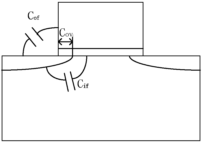
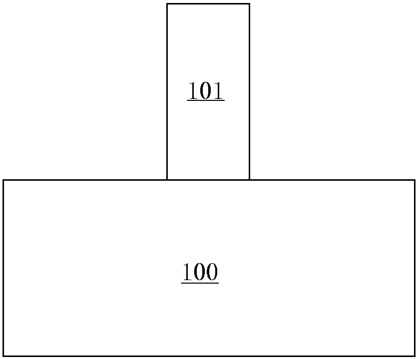
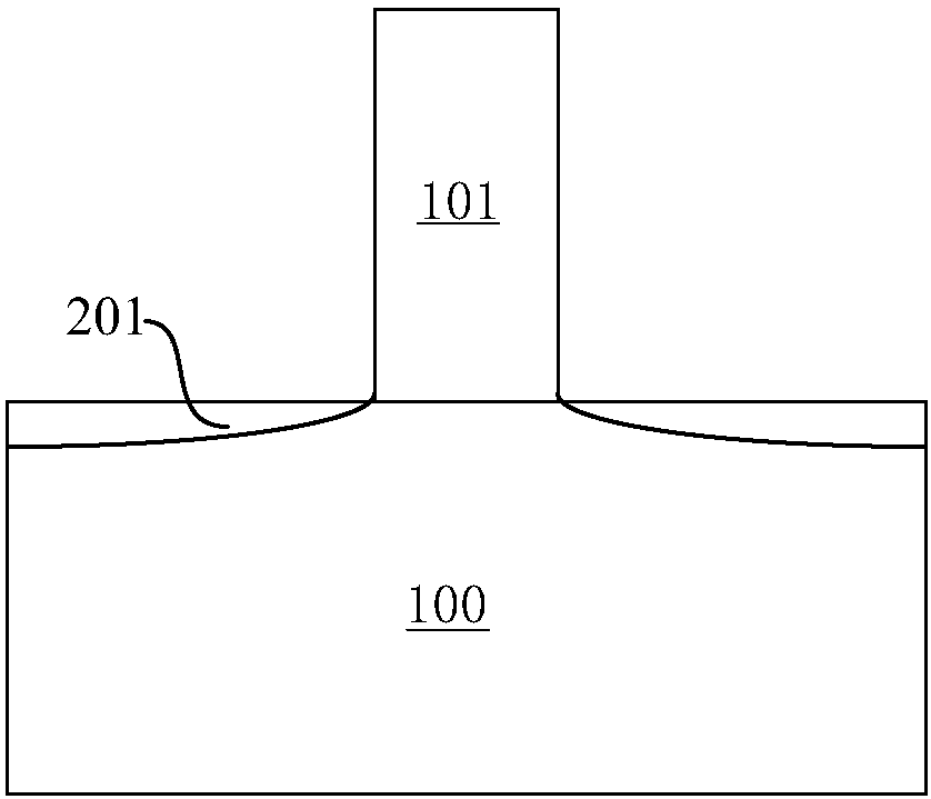
[0022] Such as Figure 15 As shown, an embodiment of the present invention provides a MOS transistor structure, including: a substrate 100; a gate stack 200 located above the substrate 100; spacers located on both sides of the gate stack 200 102 ; vacancies 340 on both sides of the spacer 102 ; an interlayer dielec...


PUM


Abstract

The invention provides a method for manufacturing a MOS transistor, comprising: a. providing a semiconductor substrate, dummy gate stacks, spacers, and source-drain regions; b. forming a first interlayer dielectric layer whose height is less than that of the dummy gate The height of the stack; c. remove the part of the first interlayer dielectric layer located at both ends away from the dummy gate stack to form a first vacancy; d. fill the second interlayer dielectric layer in the first vacancy, which The top is located between the top of the first interlayer dielectric layer and the top of the gate stack; e. forming a third interlayer dielectric layer to cover the first interlayer dielectric layer and the second interlayer dielectric layer; f. forming a through hole exposing the first interlayer dielectric layer in the interlayer dielectric layer; g. removing the first interlayer dielectric layer through the through hole to form a second vacancy; h. forming a cap layer to fill the through hole hole. The invention effectively reduces the gate parasitic capacitance and improves device performance.

Description

technical field [0001] The present invention relates to a semiconductor device structure and a manufacturing method thereof, in particular to a MOS transistor structure and a manufacturing method thereof. Background technique [0002] In the MOSFET structure, the gate parasitic capacitance is a key factor affecting the frequency response and switching speed of the device, and determines the gate RC delay and RF frequency response. In order to improve the performance of the device, we need to reduce the parasitic capacitance of the MOSFET as much as possible. As the size of the device decreases, the influence of the parasitic capacitance becomes more and more significant. Further reducing the parasitic capacitance of the device can significantly improve the performance of the device. [0003] Parasitic capacitance is directly determined by the physical structure of the device, and its size is directly related to the size of the device. Such as figure 1 As shown, the gate pa...

Claims


Application Information

Patent Timeline
Patent Type & Authority Patents(China)
IPC IPC(8): H01L21/336H01L29/78
Inventor 李睿尹海洲刘云飞
Owner 北京中科微投资管理有限责任公司
Why Eureka
Try Eureka