Horizontal electric field driving mode array substrate and touch screen

An array substrate and horizontal electric field technology, applied in the direction of electrical digital data processing, input/output process of data processing, instruments, etc., can solve problems such as touch noise, achieve the effects of reducing production costs, improving touch sensitivity, and reducing the process

Active Publication Date: 2013-08-28
SHANGHAI TIANMA MICRO ELECTRONICS CO LTD
View PDF5 Cites 35 Cited by
  • Summary
  • Abstract
  • Description
  • Claims
  • Application Information

AI Technical Summary

Problems solved by technology

[0006] Another object of the present invention is to solve the problem of touch noise generated by the liquid crystal layer of the horizontal electric field drive mode touch screen, and improve its touch sensitivity

Method used


Image

  • Horizontal electric field driving mode array substrate and touch screen
  • Horizontal electric field driving mode array substrate and touch screen
  • Horizontal electric field driving mode array substrate and touch screen

Examples


Embodiment 1

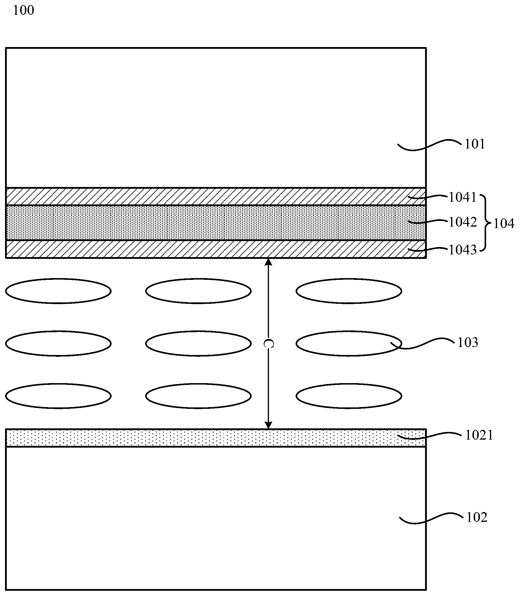
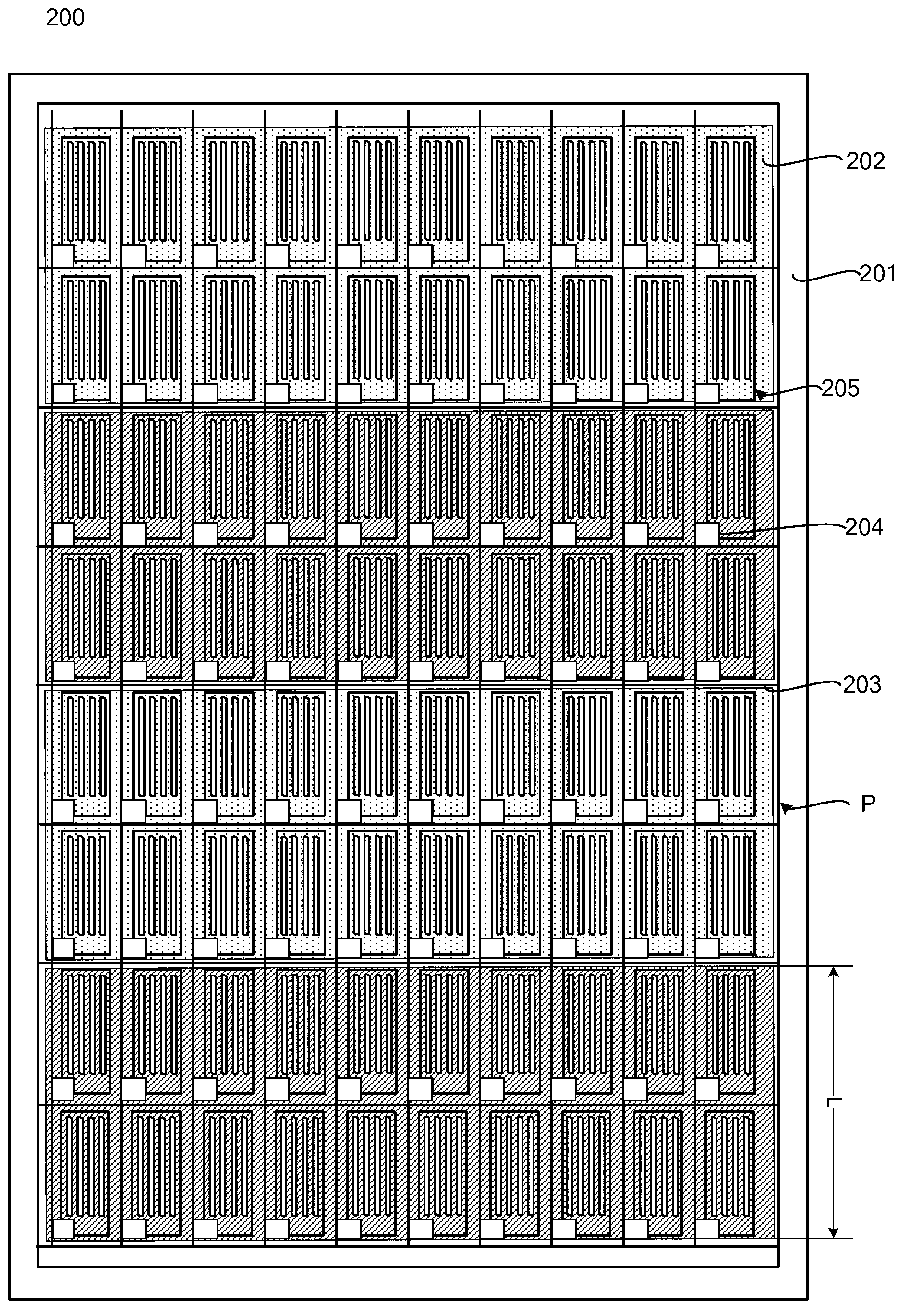
[0043] Such as figure 2 As shown, the fringe field switching mode (Fringe Field Switching, FFS) array substrate 200 of this embodiment includes a substrate 201, a plurality of common electrode lines 202 formed on the substrate 201, and a plurality of common electrode lines 202 formed on the substrate 201. A plurality of gate lines 203 and data lines 204 intersecting with the gate lines 203 , and a region defined by adjacent data lines 204 and gate lines 203 is a pixel region P. Wherein, the width L of the common electrode line 202 can be selected according to needs, for example, the width range of the common electrode line 202 is 3mm˜5mm. For the convenience of illustration, in figure 2 In , the adjacent common electrode lines 202 are represented by different filling colors.

[0044] continue to refer figure 2 , the common electrode lines 202 and the data lines 204 are vertically arranged. During the touch control period, the common electrode line 202 serves as a sensin...

Embodiment 2

[0048] As mentioned above, the idea of ​​the present invention can be applied to all array substrates in horizontal electric field driving mode. Such as Figure 5 In this embodiment, an in-plane switching mode (In-Plane Switching, IPS) array substrate 300 is provided, including a substrate 301, a plurality of common electrode lines 302 formed on the substrate 301, and a plurality of common electrode lines 302 formed on the substrate 301. A plurality of gate lines 303 and data lines 304 intersecting with the gate lines 303 above, and a region defined by adjacent data lines 304 and gate lines 303 is a pixel region P. The common electrode lines 302 are perpendicular to the data lines 304 . During the touch control period, the common electrode line 302 serves as a sensing electrode or a driving electrode for realizing a touch function, and the data line 304 serves as a driving electrode or a sensing electrode for realizing a touch function.

[0049] Such as Image 6 with Figu...

Embodiment 3

[0053] The difference between this embodiment and Embodiment 1 and Embodiment 2 is that the line widths of the common electrode lines in the two embodiments are different. The number of common electrode lines coming out is different.

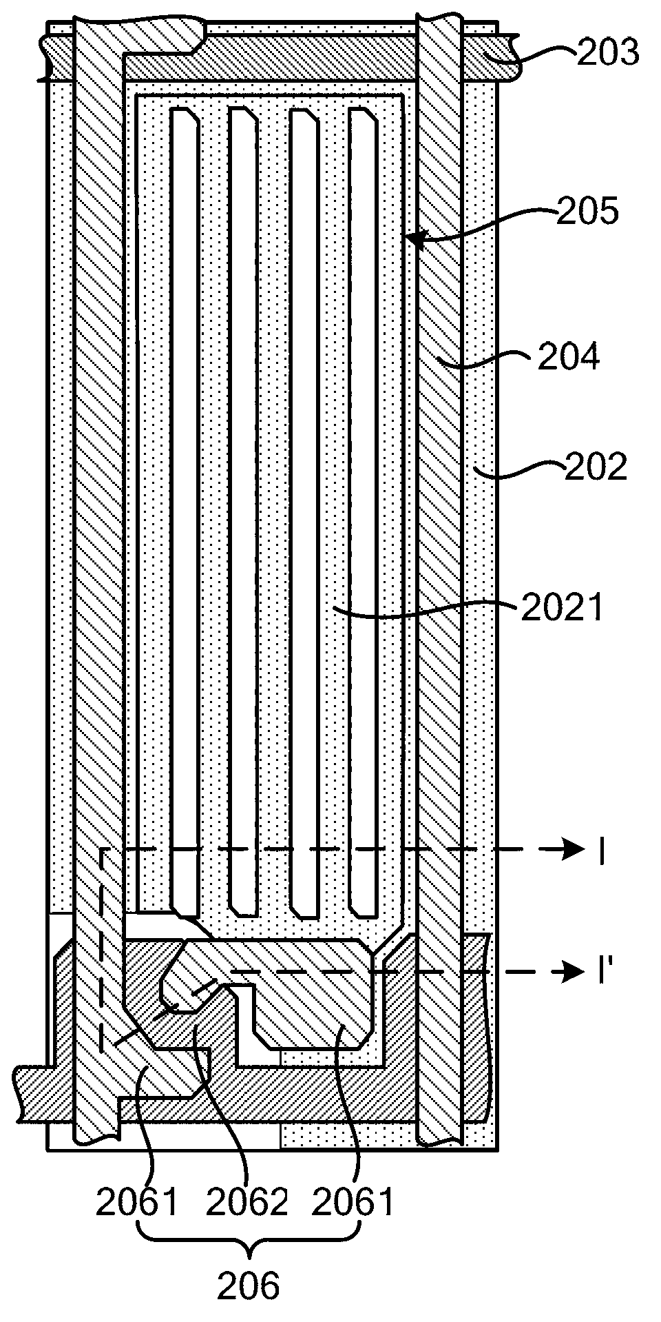
[0054] Specifically, as Figure 8 As shown, on the array substrate 200 in the horizontal electric field driving mode of this embodiment, the plurality of data lines 204 and the plurality of gate lines 203 will form a plurality of pixel rows and a plurality of pixel columns. The common electrode lines 203 are overlapped with pixel rows or pixel columns, that is, each common electrode line 203 corresponds to a pixel row.

[0055] Because each common electrode line 203 corresponds to a pixel row, when the common electrode 202 is in the display period, the touch function during the touch period will not affect its function as a storage capacitor, thereby optimizing the display effect. Moreover, when the common electrode line 203 overlaps with the ...


PUM

PropertyMeasurementUnit
widthaaaaaaaaaa

Abstract

The invention discloses a horizontal electric field driving mode array substrate and a touch screen. The horizontal electric field driving mode array substrate comprises a substrate, a plurality of pubic electrode wires, a plurality of grid electrode wires and data wires, wherein the pubic electrode wires are formed on the substrate; the grid electrode wires are formed on the substrate; the data wires are cross with the grid electrode wires; in the touch period, the pubic electrode wires are used as sensing electrodes or driving electrodes; and the data wires or the grid electrode wires are used as driving electrodes or sensing electrodes. When the horizontal electric field driving mode touch screen disclosed by the invention is adopted, the technical manufacture process can be reduced, the production cost is effectively lowered, meanwhile, touch noise caused by a liquid crystal layer can be reduced, and the touch sensitivity can be effectively improved.

Description

technical field [0001] The invention relates to flat panel display technology, in particular to an array substrate and a touch screen in a horizontal electric field driving mode. Background technique [0002] The touch screen embedded in the liquid crystal display is widely used because it can be integrated on the color filter substrate or the array substrate, which effectively reduces the thickness of the entire touch display device. For liquid crystal displays with horizontal electric field drive mode, such as fringe field switching mode (Fringe Field Switching, FFS) or in-plane switching mode (In-Plane Switching, IPS), etc., the embedded touch screen usually needs to be used to complete the touch function. Both the driving line and the sensing line are integrated on one side of the color filter substrate. [0003] Such as figure 1 As shown, the FFS in-cell touch screen 100 includes a color filter substrate 101 , an array substrate 102 , a liquid crystal layer 103 and a ...

Claims


Application Information

Patent Timeline
Patent Type & Authority Applications(China)
IPC IPC(8): G06F3/044G06F3/041G02F1/1362G02F1/1333
CPCG02F1/134363G06F3/0412G06F2203/04103G02F1/13338G06F3/0443G02F1/134372
Inventor 马骏赵丽军姚绮君
Owner SHANGHAI TIANMA MICRO ELECTRONICS CO LTD
Why Eureka
Try Eureka