Clock alignment circuit having a self regulating voltage supply

a clock alignment and voltage supply technology, applied in the field of clock alignment circuits and techniques, can solve the problems of noisy power supply, power supply noise may also introduce, power supply noise can be reduced, so as to reduce power dissipation and increase power supply noise immunity. , the effect of widening the operating rang

Inactive Publication Date: 2005-08-09
RAMBUS INC
View PDF29 Cites 154 Cited by
  • Summary
  • Abstract
  • Description
  • Claims
  • Application Information

AI Technical Summary

Benefits of technology

[0019]The present invention relates to clock alignment circuits and techniques for use in high speed integrated circuit devices, which generate clock signals having a synchronous, precisely controlled, and / or predetermined relationship with reference signals. The clock alignment circuits and techniques of the present invention exhibit wide operating range, reduced power dissipation, increased power supply noise immunity, increased immunity to noise induced jitter, and decreased process and temperature variation sensitivity.

Problems solved by technology

Large currents and fast switching of these circuits tend to induce noise on power supply systems.
Noisy power supplies tend to distort or skew a clock signal generated in, for example, a delay element in a DLL or PLL system.
Power supply noise may also introduce variations between clock cycles of internal clock signals used in the clock alignment system on an integrated circuit device.
Furthermore, substrate or ground induced noise, variations in semiconductor processing, and changing temperatures may also cause distortions in clock signals.
Noise sources and environmental effects may impose a serious limitation to the performance of clock alignment circuit designs.
However, conventional differential amplifier type delay elements tend to consume high levels of static power.
As such, these delay elements are undesirable or not compatible for use in many applications—for example applications which require low power dissipation, such as, portable battery operated applications.
Indeed, the differential amplifier type delay elements of FIG. 3 dissipates more static power than typical static inverter type elements.
Static inverter elements, while having negligible static power dissipation, tend to be much more susceptible to power supply fluctuations than differential amplifier type delay elements.
Thus, conventional clock alignment circuit employing differential elements in a delay line may provide the advantage of high noise immunity but tend to suffer from unacceptable power consumption levels.
There are a number of drawbacks in using the regulated power supply approach to improve immunity from power supply noise.
In addition, the band gap regulator 400 may consume unacceptable levels of power at low clock alignment system operating frequencies.
Moreover, a portion of the clock alignment circuitry may have to operate at a lower supply voltage, thereby adding additional design complexity.
In addition, by employing static inverter type delay elements, significant noise immunity may be realized along with negligible static power consumption penalty.
However, the dedicated pin approach may require additional area on an integrated circuit for the inclusion of an extra bond pad.
In addition, the dedicated pin approach may have limited applications.
Also, the dedicated pin approach may render the clock alignment circuitry susceptible to other sources of noise such as ground induced noise or substrate coupled noise.
Thus, in sum, although clock alignment circuits employing differential delay elements provide a relatively high noise immunity, such circuits suffer from unacceptable power consumption levels.
Static inverter elements employed in the delay line may have lower power consumption (relative to differential delay elements) but have the disadvantage of lower noise immunity.
Although noise susceptibility of the static inverter element may be improved through the use of regulated power supplies, such as a bandgap regulator, such a configuration may also impose undesirable complexity and consume excess power.
A dedicated power supply pin may solve the noise susceptibility concerns of the static inverter element, however dedicated pin designs tend to impose additional integrated circuit area requirements and may have limited applications.
The static inverter delay line element approach may offer inherent static power consumption but may otherwise exhibit poor noise susceptibility.
The regulated supply approach while providing increased noise immunity to the static inverter delay line element, may require undesirable complexity and exhibit unscalable power consumption.

Method used


Image

  • Clock alignment circuit having a self regulating voltage supply
  • Clock alignment circuit having a self regulating voltage supply
  • Clock alignment circuit having a self regulating voltage supply

Examples


Embodiment Construction

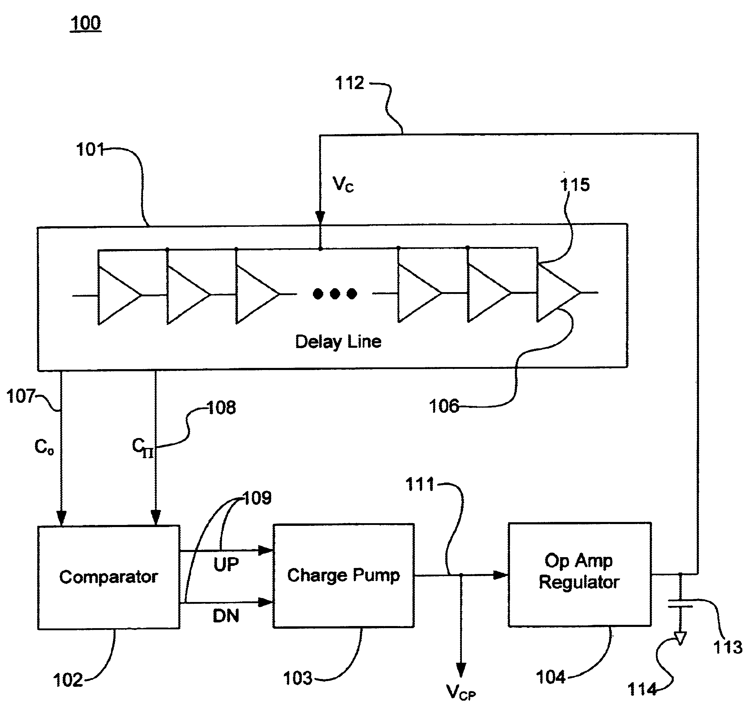
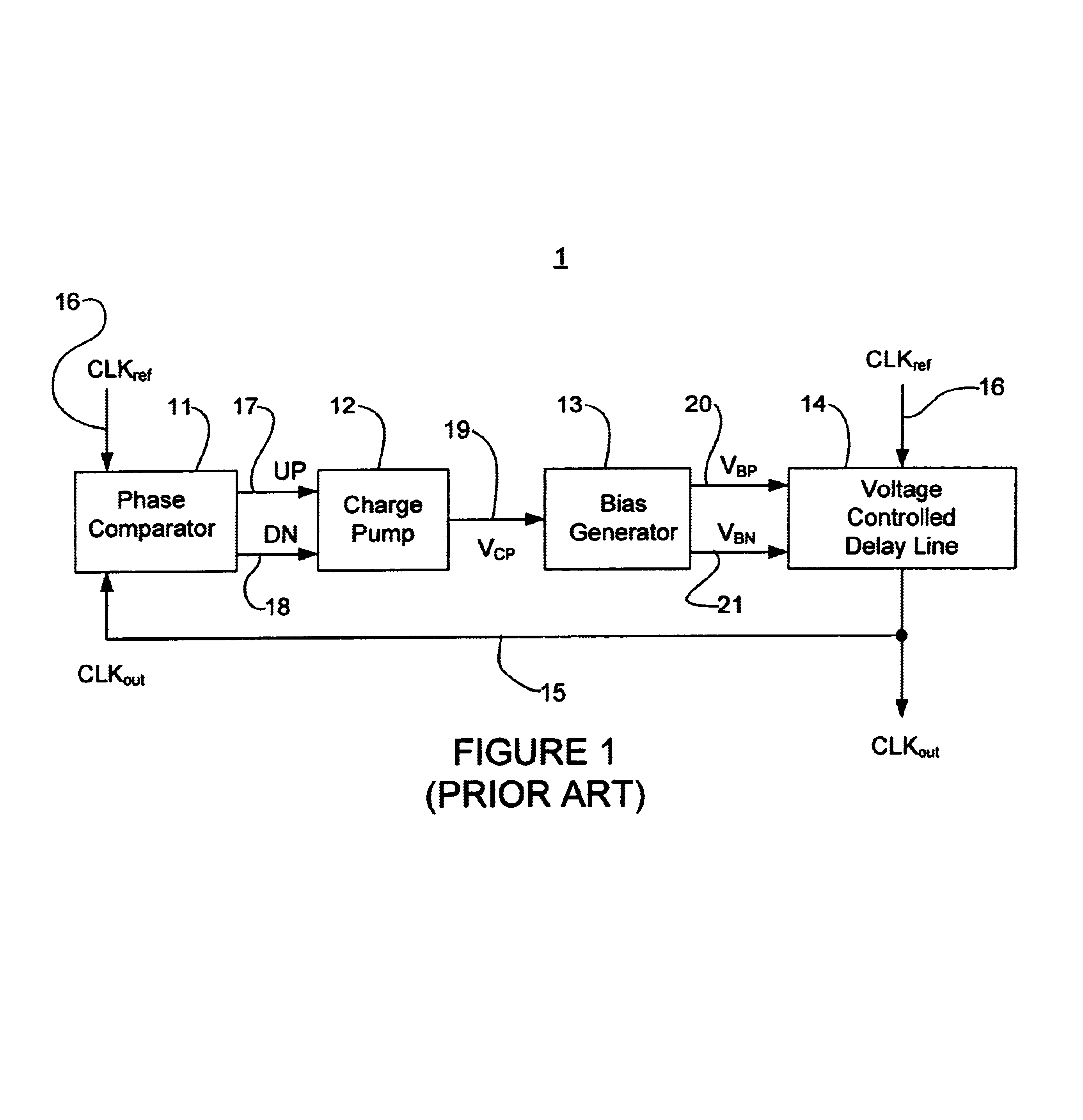
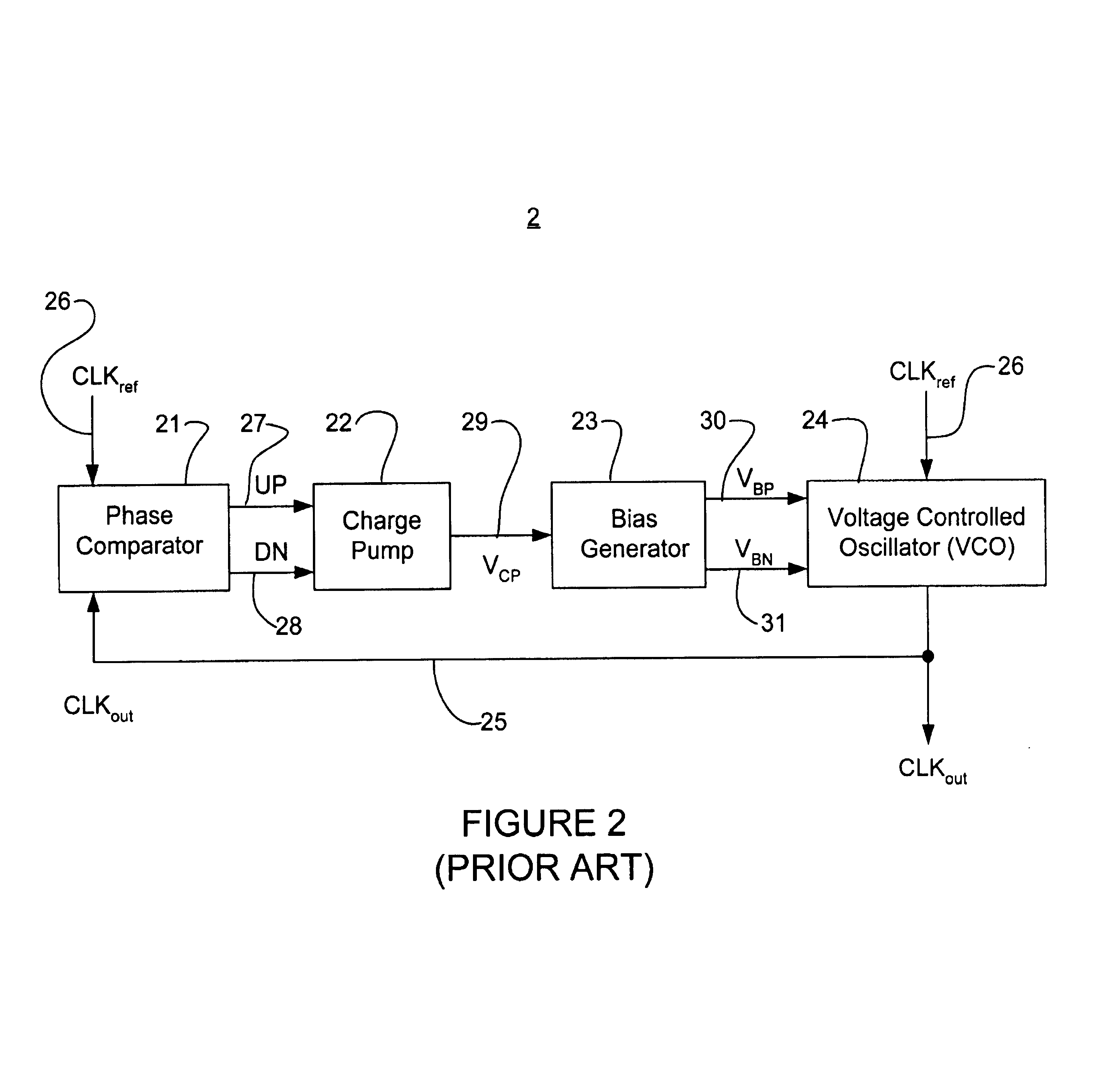
[0039]The present invention is a clock alignment circuit and technique for generating a clock signal having a defined, synchronous and / or predetermined timing relationship with respect to a reference clock signal (for example, the clock signal may be delay synchronized with the reference signal such that there is little to no delay error between the clock signal and reference clock signal or the clock signal may be frequency synchronized such that there is little to no, or negligible, phase error between the clock signal and reference clock signal). The clock alignment circuitry (or clock compensation circuitry) and technique of the present invention employs circuits and techniques to regulate the power supply voltage while providing significant immunity to power supply noise or other noise sources.

[0040]In one embodiment, a power supply circuit of the present invention is included in a feedback system of the clock alignment circuit. The power supply circuit includes an operational ...


PUM


Abstract

Clock alignment circuits and techniques for reducing power dissipation, increasing power supply noise immunity, decreasing process and temperature variation sensitivity, and providing a wide operating range. A power supply generator generates an isolated supply voltage for a delay line used in a clock alignment circuit. The delay line generates a delayed clock from a reference clock. A comparator detects a correction information (i.e., delay or phase error) between the delayed clock and the reference clock and generates error information representative of the correction information. A charge pump circuit converts the error information into a voltage signal, wherein the voltage signal is a scaled representation of the error information. The power supply generator includes an amplifier having a first input coupled to the voltage signal and an output to provide the supply voltage and a capacitor coupled between the supply voltage and a ground voltage, wherein the amplifier tracks the voltage signal level to regulate the supply voltage.

Description

BACKGROUND OF THE INVENTION[0001]This invention relates to circuits and techniques for generating clock signals which have predetermined temporal relationships with reference signals. More specifically, this invention relates to clock alignment circuits and techniques, for use in high speed integrated circuit devices, which generate clock signals having a synchronous, precisely controlled, and / or predetermined relationship with reference signals and which exhibit wide operating ranges in clock alignment, reduced power dissipation, increased power supply noise immunity, and decreased process and temperature variation sensitivity.[0002]Clock alignment circuits are required in many of today's high speed integrated circuit devices to generate a clock signal having a certain timing relationship with a reference signal. In short, clock alignment circuits are employed to generate clock signals having a synchronous, precisely controlled, and / or predetermined relationship with a reference si...

Claims


Application Information

Patent Timeline
Patent Type & Authority Patents(United States)
IPC IPC(8): H03D3/00H03D3/24H03K5/00H03K5/13H03L7/081H03L7/089
CPCH03K5/133H03L7/0812H03L7/0896H03K2005/00026
Inventor SIDIROPOULOS, STEFANOS
Owner RAMBUS INC
Why Eureka
Try Eureka