Light emitting device

a technology of light emitting elements and light sources, which is applied in the direction of semiconductor devices for light sources, lighting and heating apparatus, and light support devices, etc., can solve the problems of detachment of the light emitting element from the flexible substrate, and deterioration of the light emitting element itself, so as to achieve the effect of minimizing the stress on the light emitting elemen

Active Publication Date: 2016-07-07
NICHIA CORP
View PDF1 Cites 2 Cited by
  • Summary
  • Abstract
  • Description
  • Claims
  • Application Information

AI Technical Summary

Benefits of technology

This patent is for a light emitting device that reduces stress on the light emitting element. The technical effect is that this device minimizes the stress placed on the light emitting element, resulting in improved performance and reliability.

Problems solved by technology

In the case where the adhesive layer and / or the magnet tape is disposed on the whole surface of the back surface side of the substrate, particularly on the back surface side of the substrate which is the opposite side from the region where the at least one light emitting element is mounted, and in the case where such a light emitting device is installed on a mounting substrate or various locations, due to the adhesion layer, the light emitting element itself, together with the flexible substrate, will be fixed to the mounting substrate, which may result in a stress on the light emitting element.
This may result in failures such as deterioration of the light emitting element itself and detachment of the light emitting element from the flexible substrate.

Method used


Image

  • Light emitting device
  • Light emitting device
  • Light emitting device

Examples


embodiment 1

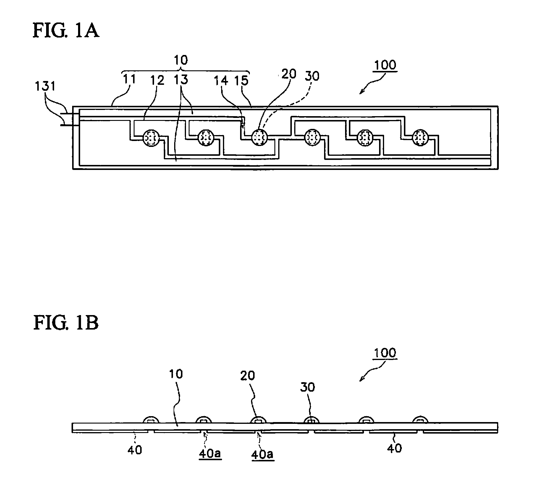
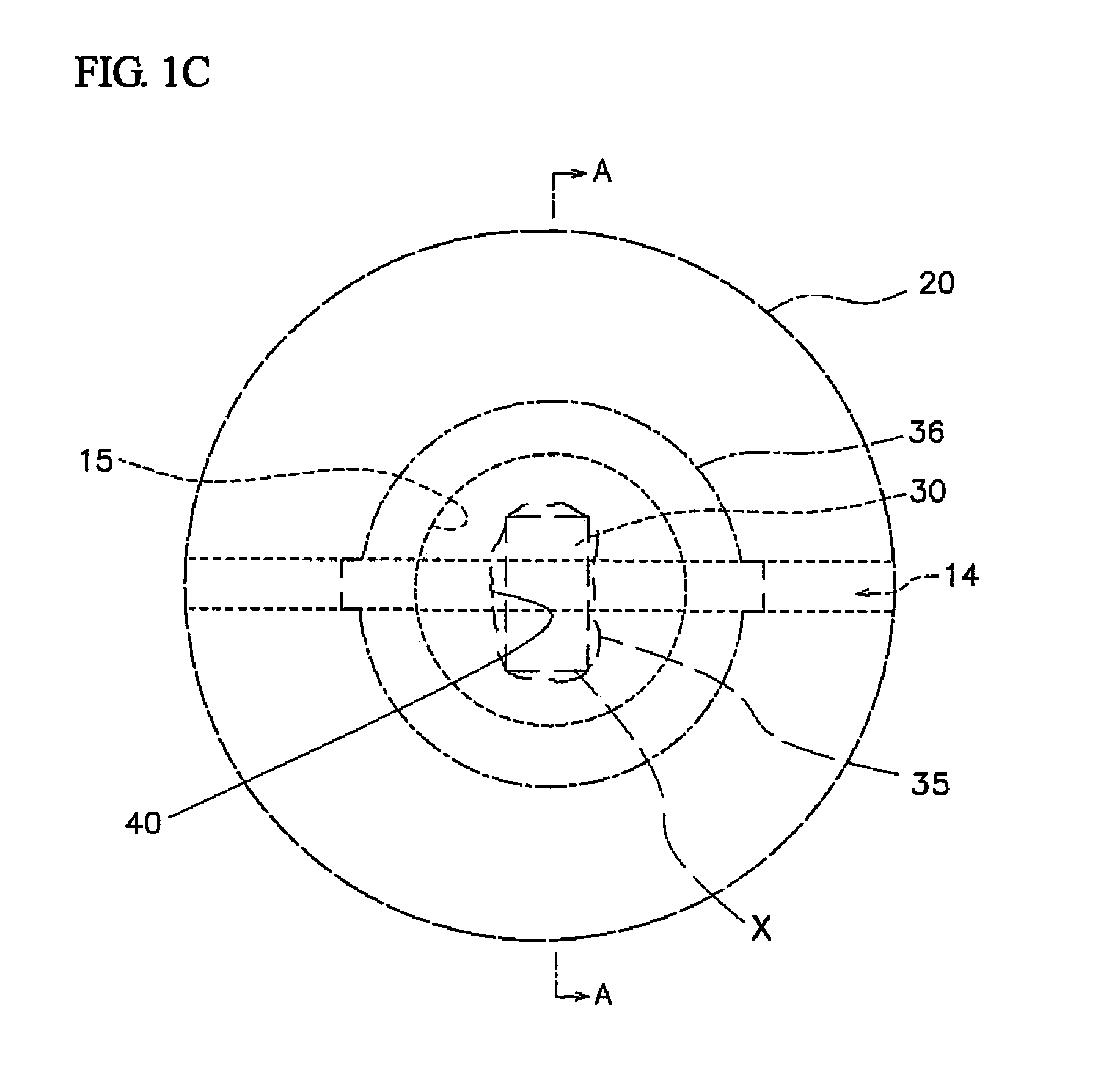
[0056]The light emitting device 100 according to Embodiment 1 includes, as shown in FIG. 1A to FIG. 1D, the flexible substrate 10, the light emitting elements 30 arranged on the surface of the flexible substrate 10, the sealing resin members 20 which are disposed on the flexible substrate 10 and cover the respective light emitting elements 30, and the adhesion layer 40. The flexible substrate 10 has a stacked layer structure made up of a flexible base member 11 made of a polyimide (about 25 μm thickness), wiring portions 12 (about 35 μm thickness) arranged on one surface of the base member 11 and spaced apart from each other by a groove portion 14, and an insulating reflective layer 15 (about 15 μm thickness and made of a silicone-system resin containing titanium oxide) disposed over them. In the flexible substrate 10, in order to establish electrical connection with the light emitting elements 30, a grove portion 14 formed between the wiring portions 12 and the wiring portions 12 a...

embodiment 2

[0065]The light emitting device 200 according to Embodiment 2 has a substantially similar structure as that of the light emitting device 100 except that, for example, as a structure shown in FIG. 2, the structure includes on the back surface of the flexible substrate 10, the separation layer 50 made of silicone is formed in the through holes 40a of the adhesion layer. The separation layer 50 is formed with a thickness approximately similar to the thickness of the adhesion layer 40.

[0066]Such a separation layer portions 50 are disposed, for example, such that a mask having openings in regions correspond to the regions X described above is prepared and placed on the back surface of the flexible substrate 10 so that the openings of the mask are aligned correspond to the regions X. Next, using the mask, by way of coating, the separation layer portions are formed on the back surface of the flexible substrate 10 at locations corresponding to the regions X. Then, the adhesion layer 40 is c...

embodiment 3

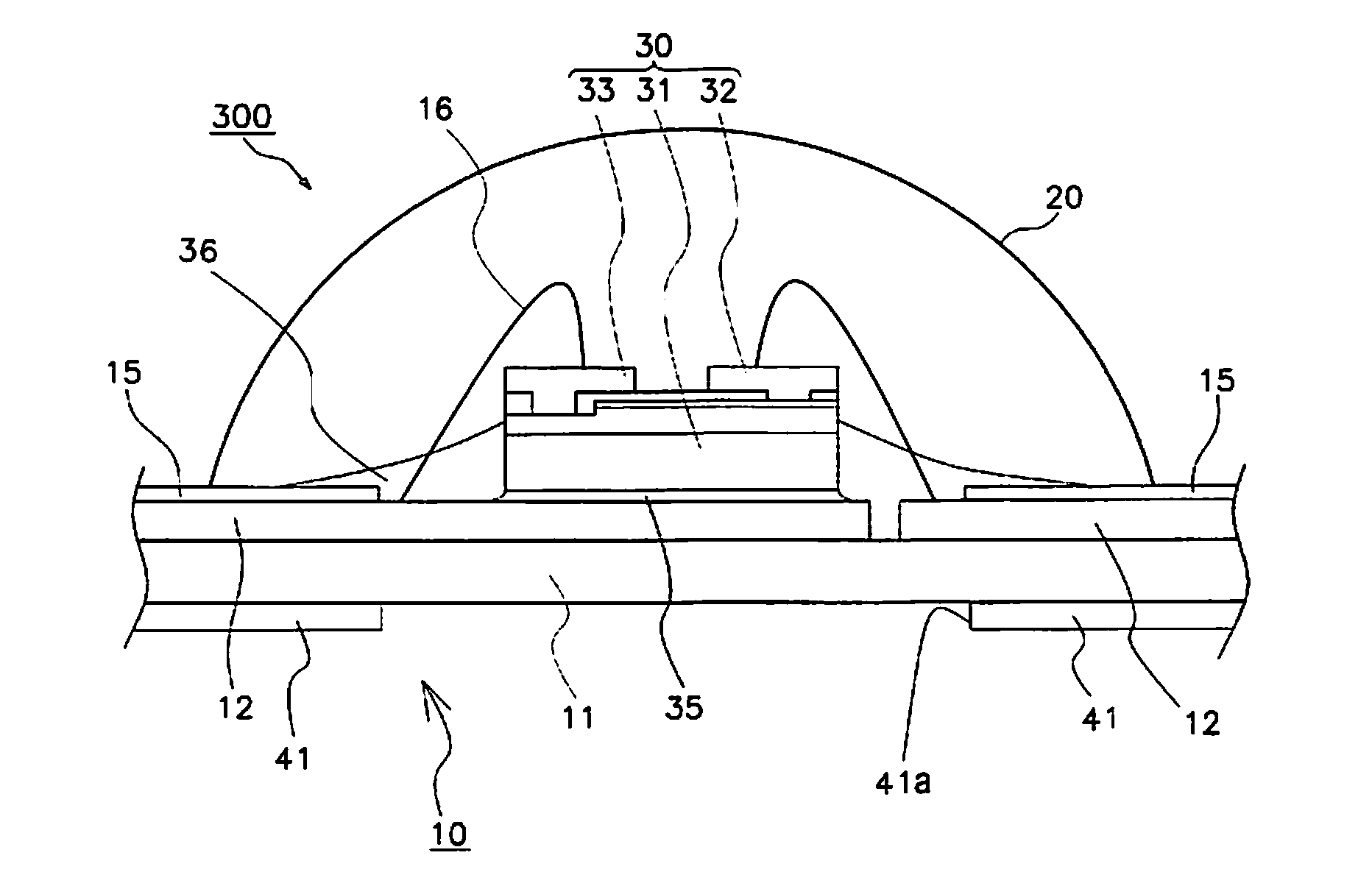
[0070]The light emitting device 300 according to Embodiment 3 has a substantially similar structure as that of the light emitting device 100 except that, as a structure shown in FIG. 3, each of the light emitting elements 30 is mounted on the wiring portions 12 of the flexible substrate 10 in a face-up manner, the n-side electrode and the p-side electrode 32 are respectively electrically connected to the corresponding wiring portions 12 via respective wires 16. Thus, on the flexible substrate 10, the region where the wiring portions 12 being exposed from the reflective layer 15 is somewhat increased, the connection regions of the wires 16 and the wiring portions 12 are also included in the corresponding region on the backside surface of the flexible substrate 10 in the similar manner as in the regions where the light emitting elements are arranged, and accordingly, the size of the through holes 41a of the adhesion layer 41 of the flexible substrate 10 are increased. That is, the adh...


PUM


Abstract

A light emitting device includes a flexible substrate, at least one light emitting element, a sealing resin and an adhesion layer. The flexible substrate includes a flexible base member and a plurality of wiring portions disposed on one surface of the base member. At least one light emitting element is arranged on a first surface of the flexible substrate and electrically connected to the wiring portions. The sealing resin seals the light emitting element. The adhesion layer is arranged on a second surface of the flexible substrate different from the first surface of the flexible substrate. The adhesion layer has a non-adhesive region corresponding at least to a region on the first surface where the at least one light emitting element is arranged. The non-adhesive region is covered with a non-adhesive layer.

Description

CROSS-REFERENCE TO RELATED APPLICATIONS[0001]This is a divisional application of U.S. patent application Ser. No. 14 / 025,962 filed on Sep. 13, 2013. This application claims priority to Japanese Patent Application No. 2012-202952 filed on Sep. 14, 2012. The entire disclosures of U.S. patent application Ser. No. 14 / 025,962 and Japanese Patent Application No. 2012-202952 are hereby incorporated herein by reference.BACKGROUND OF THE INVENTION[0002]1. Field of the Invention[0003]The present invention relates to a light emitting device which includes a flexible substrate and at least one light emitting element.[0004]2. Discussion of the Related Art[0005]A light emitting device has been proposed in which a light emitting device having at least one light emitting element is arranged on a flexible substrate. Such a light emitting device includes an adhesive layer or a magnet tape on a back surface side of the flexible substrate so that the device can be installed on various places such as a ...

Claims


Application Information

Patent Timeline
Patent Type & Authority Applications(United States)
IPC IPC(8): H01L33/56H01L33/62H01L33/08
CPCH01L33/56H01L33/62H01L33/08H01L33/486H01L25/0753H01L2224/73204H01L2224/73265H01L2224/48091H01L2924/00014H01L33/54H05K1/189H05K3/0061H05K2201/10106F21V21/0808F21S4/24F21Y2103/10F21Y2115/10F21Y2101/00H01L33/44
Inventor YAMADA, MOTOKAZU
Owner NICHIA CORP
Why Eureka
Try Eureka