Quick change small footprint testing system and method of use

a small footprint, testing system technology, applied in electrical testing, measurement devices, instruments, etc., can solve the problems of inability to test a plurality of semiconductor chips, limited cleanroom space, and high cost of dedicated testing machines for each type of chip, so as to reduce the space needed in cleanrooms, quickly and easily remove and replace, the effect of reducing capital equipment costs

Active Publication Date: 2016-07-21
MODUS TEST
View PDF0 Cites 8 Cited by
  • Summary
  • Abstract
  • Description
  • Claims
  • Application Information

AI Technical Summary

Benefits of technology

[0020]A testing system is presented having a bottom plate, a frame member and a socket plate. The socket plate holds and the frame member houses a plurality of electrical testing components therein. A removable device under test (DUT) printed circuit board (PCB) is placed on top of the socket plate and electrically connects with the electrical testing components. A removable top plate is placed on top of the DUT PCB and is locked in place by a plurality of locking posts connected to...

Problems solved by technology

The DUT PCB and testing sockets are generally custom made to fit each specific semiconductor chip, making them quite expensive.
Since cleanroom space is extremely limited it is undesirable to have a dedicated testing machine for each type of semiconductor chip.
In addition, having a d...

Method used


Image

  • Quick change small footprint testing system and method of use
  • Quick change small footprint testing system and method of use
  • Quick change small footprint testing system and method of use

Examples


Embodiment Construction

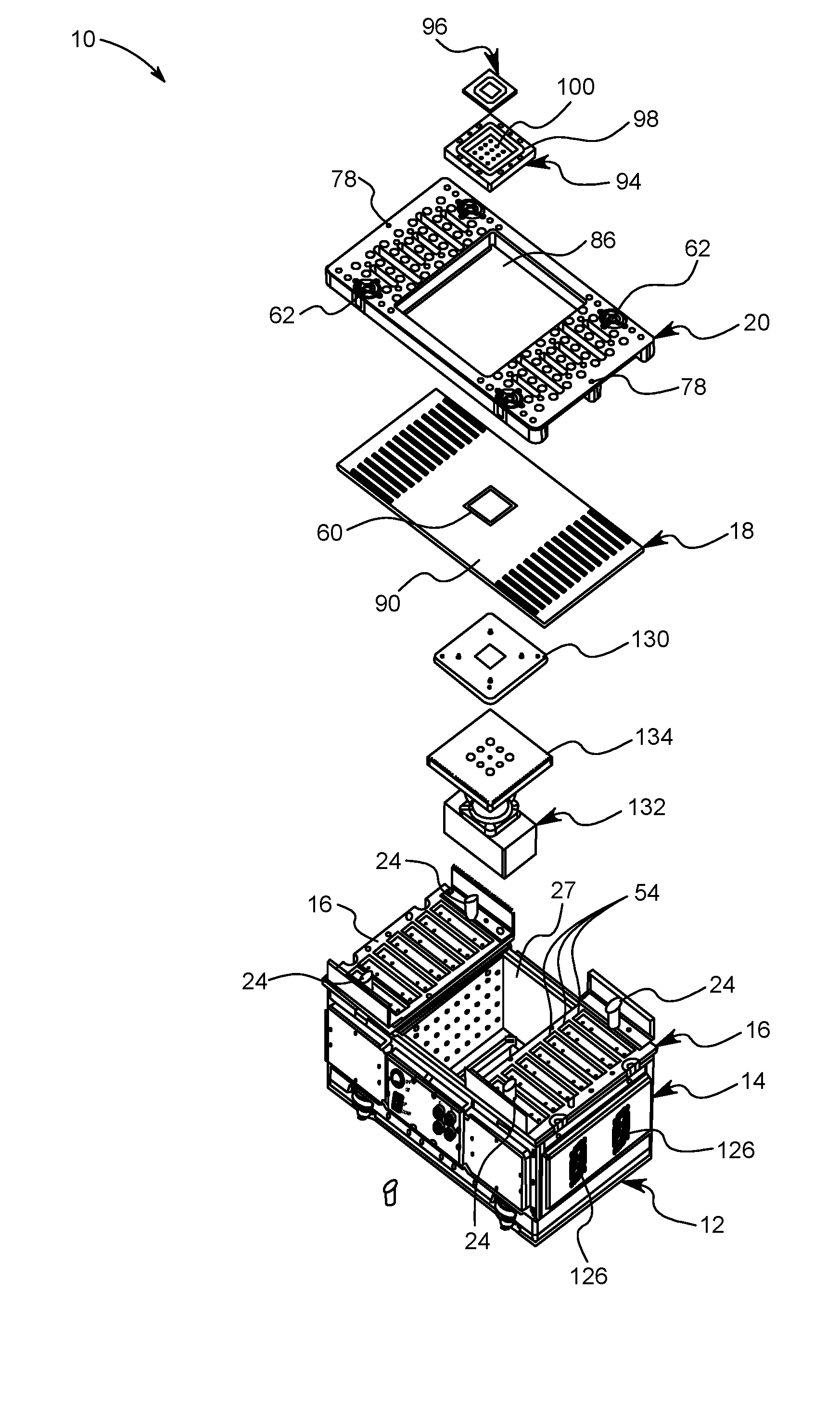
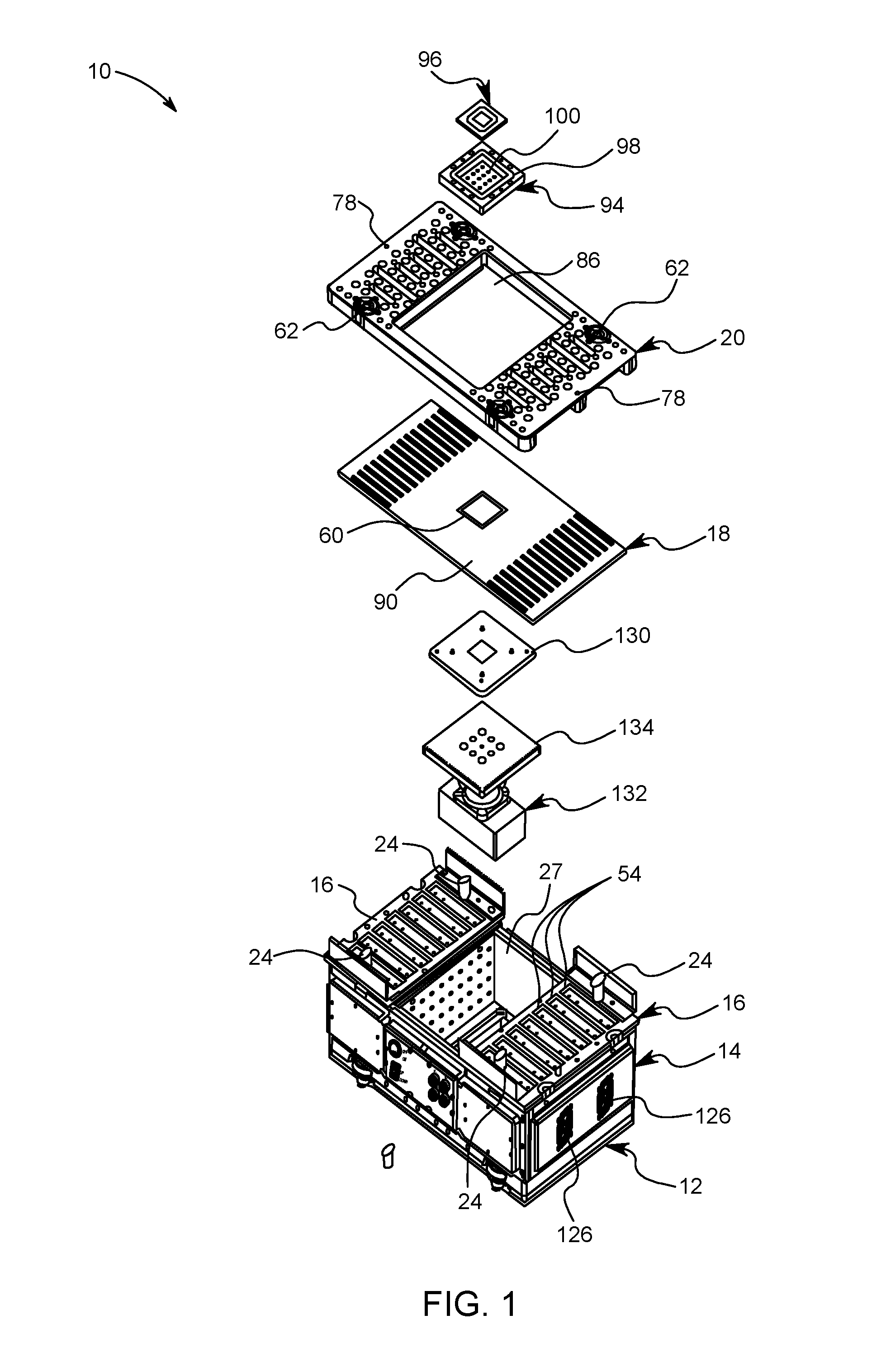
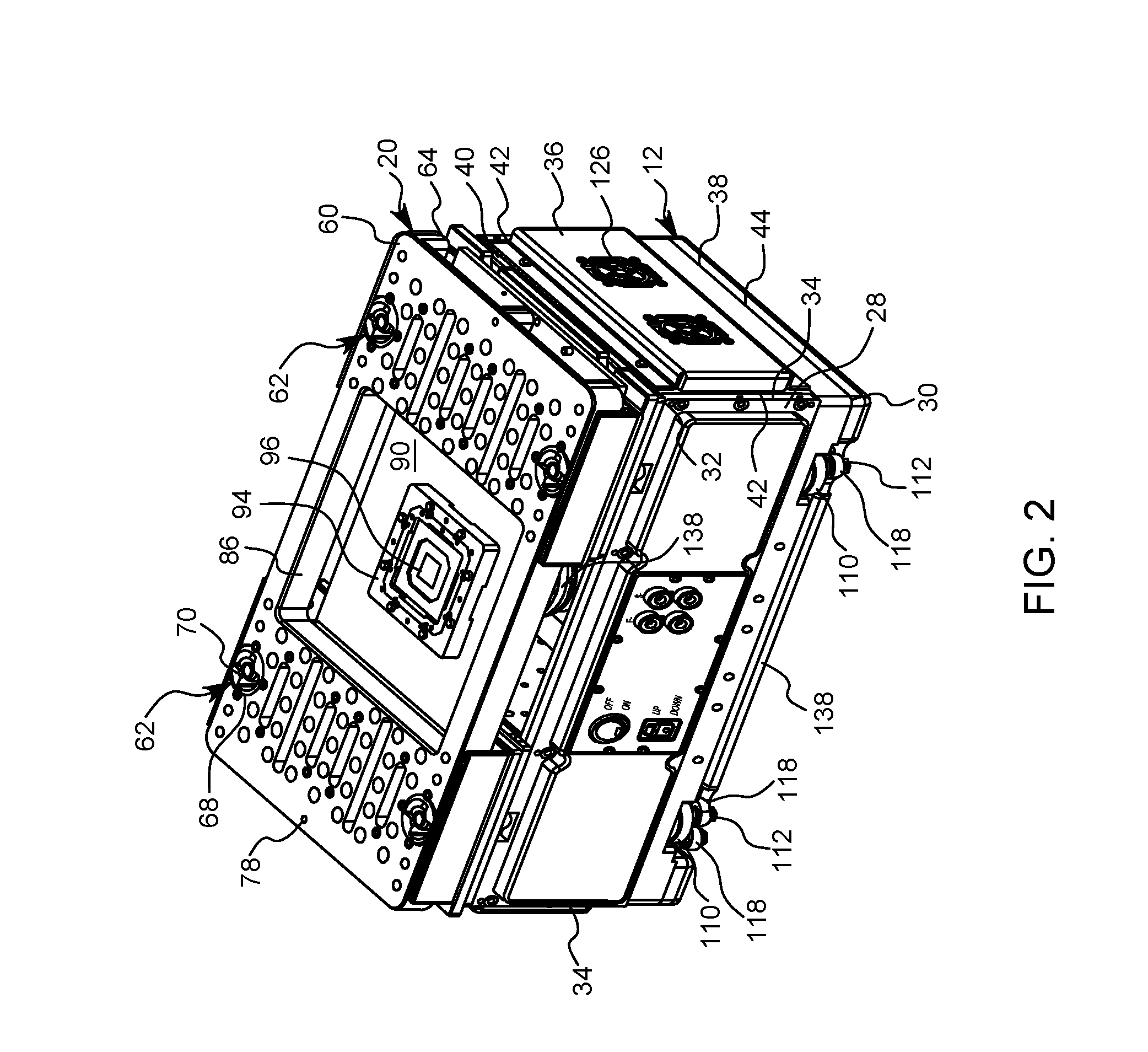
[0045]In the following detailed description, reference is made to the accompanying drawings which form a part hereof, and in which is shown by way of illustration specific embodiments in which the invention may be practiced. These embodiments are described in sufficient detail to enable those skilled in the art to practice the invention, and it is to be understood that other embodiments may be utilized and that mechanical, procedural, and other changes may be made without departing from the spirit and scope of the invention(s). The following detailed description is, therefore, not to be taken in a limiting sense, and the scope of the invention(s) is defined only by the appended claims, along with the full scope of equivalents to which such claims are entitled.

[0046]As used herein, the terminology such as vertical, horizontal, top, bottom, front, back, end, sides and the like are referenced according to the views, pieces and figures presented. It should be understood, however, that t...


PUM


Abstract

A testing system for semiconductor chips having a removable device under test printed circuit board (DUT PCB) that electrically connects with the electrical testing components of the system. A removable top plate is placed on top of the DUT PCB and is locked in place by a plurality of locking posts that selectively connect to cam surfaces in the top plate that pull the top plate down sandwiching the DUT PCB between the top plate and the electrical testing components of the system. The DUT PCB is quickly and easily removed and replaced by moving the locking posts between an engaged position and a disengaged position. In this way, a single testing system can be used to test a great variety of semiconductor chips thereby reducing capital equipment costs and space needed in cleanrooms.

Description

FIELD OF THE INVENTION[0001]This invention relates to a testing system. More specifically and without limitation, this invention relates to a testing system for semiconductor chips, and related method of use.BACKGROUND OF THE INVENTION[0002]Along with the development of semiconductor chips, a need developed to test these semiconductor chips to ensure that they are manufactured within specified tolerances and function properly. Many manufacturers of semiconductor chips such as Intel®, AMD®, Xilinx®, Texas Instruments®, NVIDIA®, Qualcomm® among countless others manufacture semiconductor chips which are then tested by a chip testing system having a device under test printed circuit board (DUT PCB) with a testing socket that is attached thereto. The DUT PCB and testing sockets are generally custom made to fit each specific semiconductor chip, making them quite expensive.[0003]Manufacturers tend to simultaneously manufacture a variety of semiconductor chips within their facilities so as ...

Claims


Application Information

Patent Timeline
IPC IPC(8): G01R1/04G01R31/26
CPCG01R31/2601G01R1/0441G01R1/0466G01R1/07328G01R1/07314G01R31/2879G01R31/2886G01R31/2889G01R31/2896
Inventor ADAMS, LYNWOODLEWIS, JACK
Owner MODUS TEST
Why Eureka
Try Eureka