Housing, manufacturing method thereof, and electronic device having the housing

a manufacturing method and housing technology, applied in the field of electronic devices, can solve the problems of increasing manufacturing costs due to the addition of components, affecting the performance of antenna radiation, and securing a space, so as to maximize the performance of the antenna

Active Publication Date: 2016-08-11
SAMSUNG ELECTRONICS CO LTD
View PDF22 Cites 48 Cited by
  • Summary
  • Abstract
  • Description
  • Claims
  • Application Information

AI Technical Summary

Benefits of technology

[0013]Accordingly, another aspect of the present disclosure is to provide a housing that may implement conducting and insulating effects at a desired position merely by a process of insert molding and processing a non-metal member to a metal member.
[0014]Accordingly, another aspect of the present disclosure is to provide a housing that is implemented such that an antenna performance is maximized by securing a mounting space and a degree of freedom of the pattern of an antenna radiator.

Problems solved by technology

However, a problem may occur in securing a space that is essentially needed for the pattern shift.
However, a housing structure using such a press-fitting pin requires an additional process of applying an additional component, and may cause degradation of the radiation performance of an antenna due to a deviation or an error that is caused as a result of assembly.
Additionally, such housing structures generally face the following problems: an increase in manufacturing costs due to the added component; the press-fitting pins may not be able to be applied to a complicated structural portion of the housing structure, such as a curved face; and a peripheral portion, around the housing structure, may be scratched or deformed in the process of press-fitting.
In addition, a conventional screw fastening structure may present electric shock problems.
For example, with a conventional screw an internal current may be transferred to an external metal housing through the screw, thereby being exposed to electric shock.
In order to prevent this, a capacitor may be arranged around the screw as an electric safety device, which may also increases unit price, and a separate mounting space is needed by adopting an additional component.

Method used


Image

  • Housing, manufacturing method thereof, and electronic device having the housing
  • Housing, manufacturing method thereof, and electronic device having the housing
  • Housing, manufacturing method thereof, and electronic device having the housing

Examples


Embodiment Construction

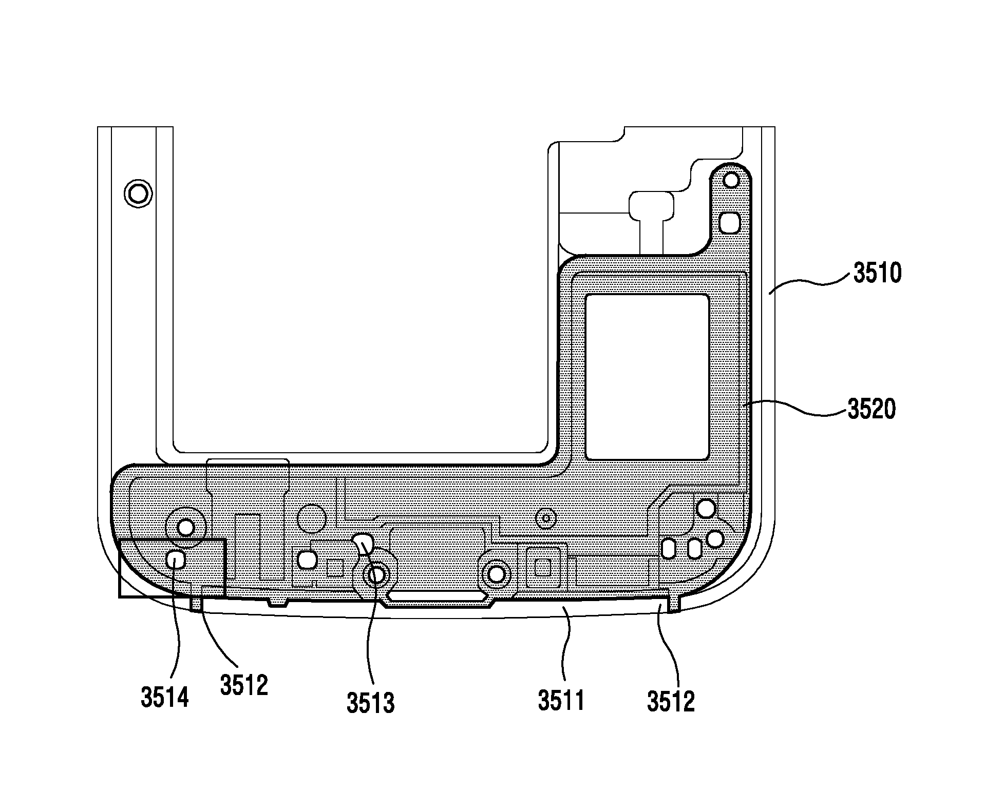
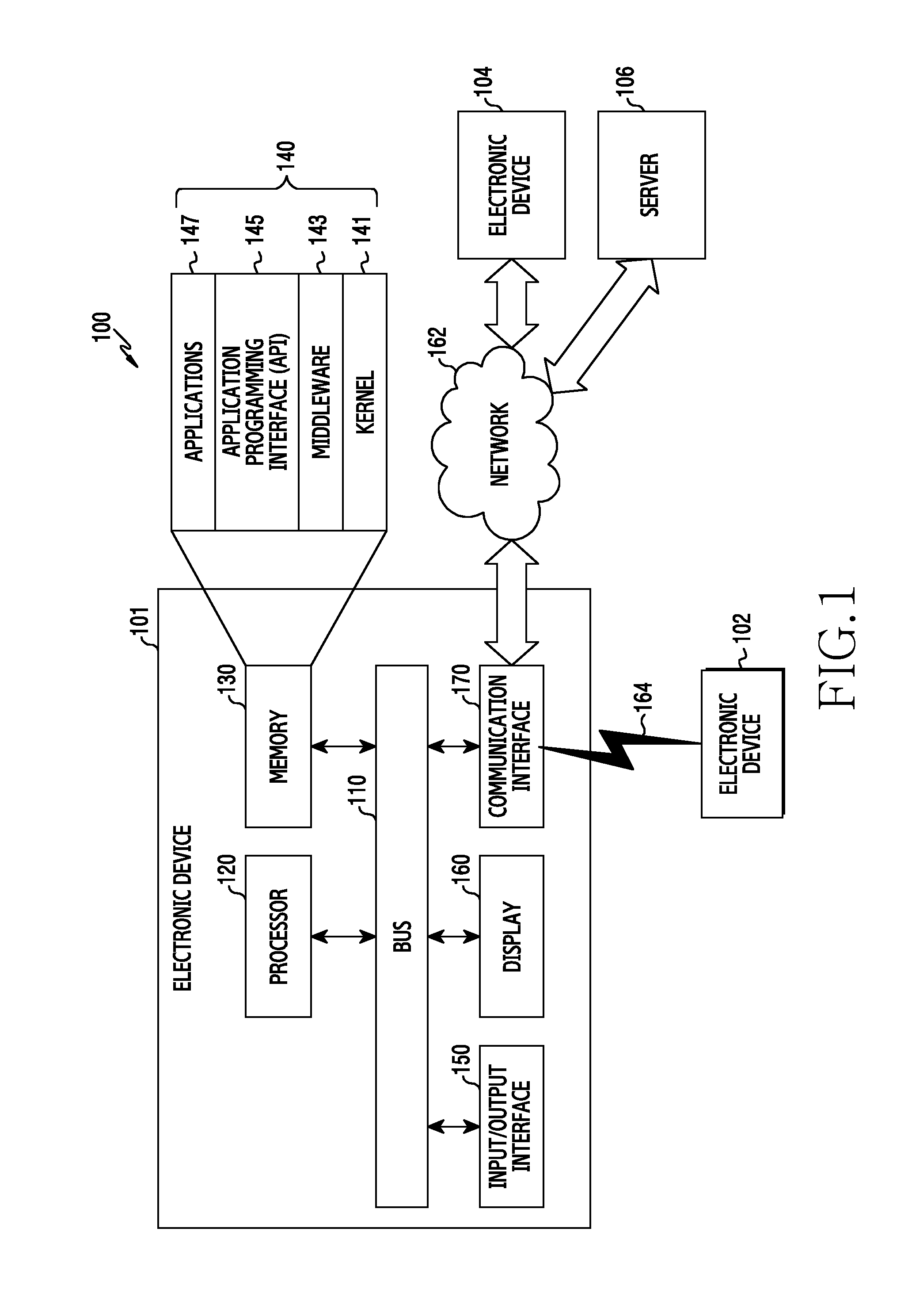
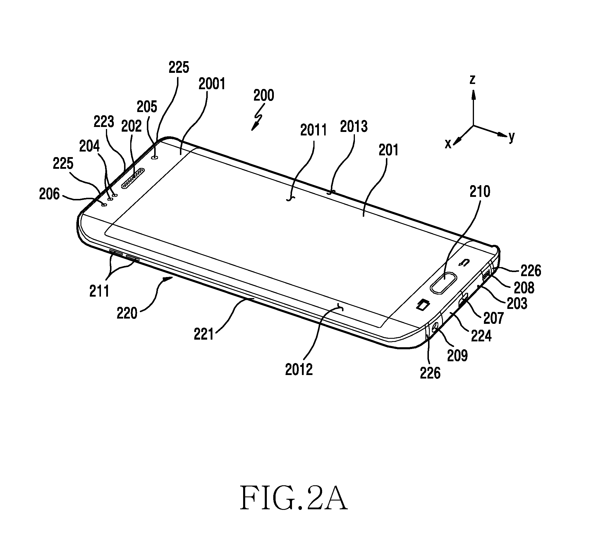
[0033]The following description with reference to the accompanying drawings is provided to assist in a comprehensive understanding of various embodiments of the present disclosure as defined by the claims and their equivalents. It includes various specific details to assist in that understanding but these are to be regarded as mere examples. Accordingly, those of ordinary skill in the art will recognize that various changes and modifications of the various embodiments described herein can be made without departing from the scope and spirit of the present disclosure. In addition, descriptions of well-known functions and constructions may be omitted for clarity and conciseness. In describing the drawings, similar reference numerals designate similar constituent elements.

[0034]The terms and words used in the following description and claims are not limited to their dictionary meanings, but are merely used to enable a clear and consistent understanding of the present disclosure. Accordi...


PUM


Abstract

A portable electronic device and a method for manufacturing the same are provided. The portable electronic device includes a front cover that forms a front face of the electronic device, a rear cover that forms a rear face of the electronic device, a bezel that surrounds a space formed by the front cover and the rear cover, a display device that is embedded in the space and includes a screen region that is exposed through the front cover, a metal structure that is positioned within the space, and includes a first face facing the front cover and a second face facing the rear cover, a non-metal structure that is positioned within the space to partially overlap with the metal structure, and includes a first surface facing the front cover and a second surface facing the rear cover, and a metal filler extending from the first surface to the second surface of the non-metal structure through a portion of the non-metal structure. The metal filler is formed of a material that is equal in strength to that of the metal structure, and includes a first end portion adjacent to the first surface and a second end portion adjacent to the second surface, and at least one of the first end portion and the second end portion are aligned to be coplanar with a portion of the first surface and a portion of the second surface, respectively.

Description

PRIORITY[0001]This application claims priority under 35 U.S.C. §119(e) to U.S. Provisional Patent Application Ser. No. 62 / 113,108 filed in the United States Patent and Trademark Office on Feb. 6, 2015, and under 35 U.S.C. §119(a) to Korean Patent Application No. 10-2015-0060745 filed in the Korean Intellectual Property Office on Apr. 29, 2015, the entire contents of each of which are incorporated herein by reference.BACKGROUND[0002]1. Field of the Disclosure[0003]The present disclosure relates generally to an electronic device, and more particularly to a housing, a method for manufacturing the housing, and an electronic device including the housing.[0004]2. Description of the Related Art[0005]As the functional differences between electronic devices of different manufacturers have recently been greatly reduced, manufacturers have gradually begun to develop slimmer electric devices in order to satisfy consumers' purchasing needs. Further, manufacturers are developing electronic device...

Claims


Application Information

Patent Timeline
Patent Type & Authority Applications(United States)
IPC IPC(8): H01Q1/24H05K5/03H05K13/00H05K5/00H01Q1/42H01Q9/04
CPCH04Q1/116H04M1/0202H01Q1/243H05K13/0023H01Q9/04H05K5/0017H05K5/03H01Q1/42H04B1/3888H05K5/0247H05K13/00H01Q9/42
Inventor SON, KWONHOBAEK, SANGINCHOI, BONGSUKKIM, GYEONGTAELEE, MINSUNG
Owner SAMSUNG ELECTRONICS CO LTD
Why Eureka
Try Eureka