Patch antenna

a technology of patch antenna and antenna body, which is applied in the direction of antennas, electrically short antennas, electrical apparatus, etc., can solve the problems of reducing antenna characteristics (e.g., gain), reducing permittivity and loss, and maximizing antenna performance. , the effect of enhancing antenna performan

Active Publication Date: 2020-10-01
AMOTECH +1
View PDF0 Cites 1 Cited by
  • Summary
  • Abstract
  • Description
  • Claims
  • Application Information

AI Technical Summary

Benefits of technology

[0015]According to the present disclosure, it is possible for the patch antenna to form the air gap between the dielectric layer and the printed circuit board, thus implementing lightweight while maximizing antenna performance. That is, the air gap has low permittivity and loss, such that it is possible for the patch antenna to enhance antenna performance, and to reduce the volume of the dielectric layer, thus implementing lightweight.
[0016]In addition, it is possible, for the patch antenna to increase the power density in the radio wave reception region as compared with the conventional patch antenna as a gain increases, thus improving a reception rate.
[0017]In addition, it is possible for the patch antenna to form the air gap that is lighter than the materials used as the dielectric layer, thus reducing the weight to implement lightweight.

Problems solved by technology

However, there is a problem in that when a dielectric layer is made of a material having a high permittivity, a patch antenna can become smaller in size and lightweight, but the antenna characteristic (e.g., gain) is reduced.

Method used


Image

  • Patch antenna
  • Patch antenna
  • Patch antenna

Examples


Embodiment Construction

[0022]Hereinafter, the most preferred embodiment of the present disclosure will be described with reference to the accompanying drawings so that those skilled in the art to which the present disclosure pertains can easily practice the technical spirit of the present disclosure. First, in adding reference numerals to the components in each drawing, it is to be noted that the same components are denoted by the same reference numerals even though they are illustrated in different drawings. In addition, in the following description of the present disclosure, a detailed description of known configurations or functions will be omitted when it is determined to obscure the subject matter of the present disclosure.

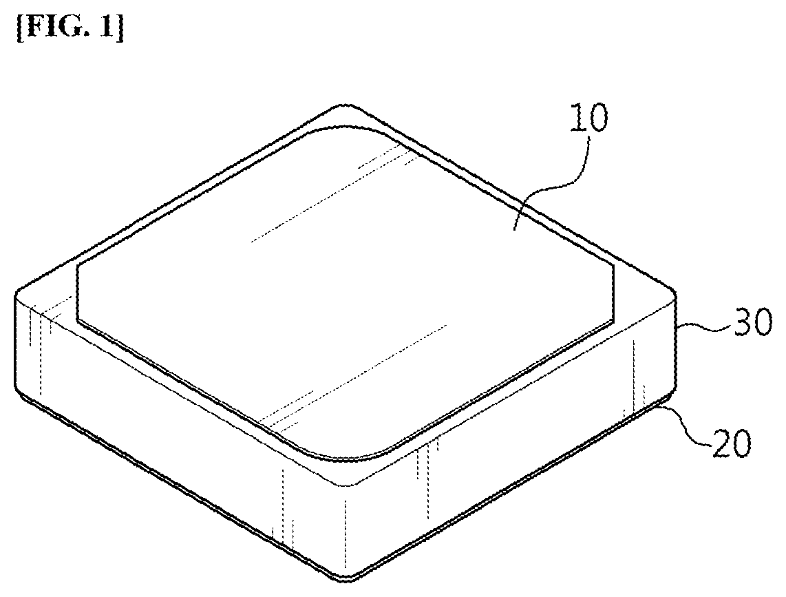
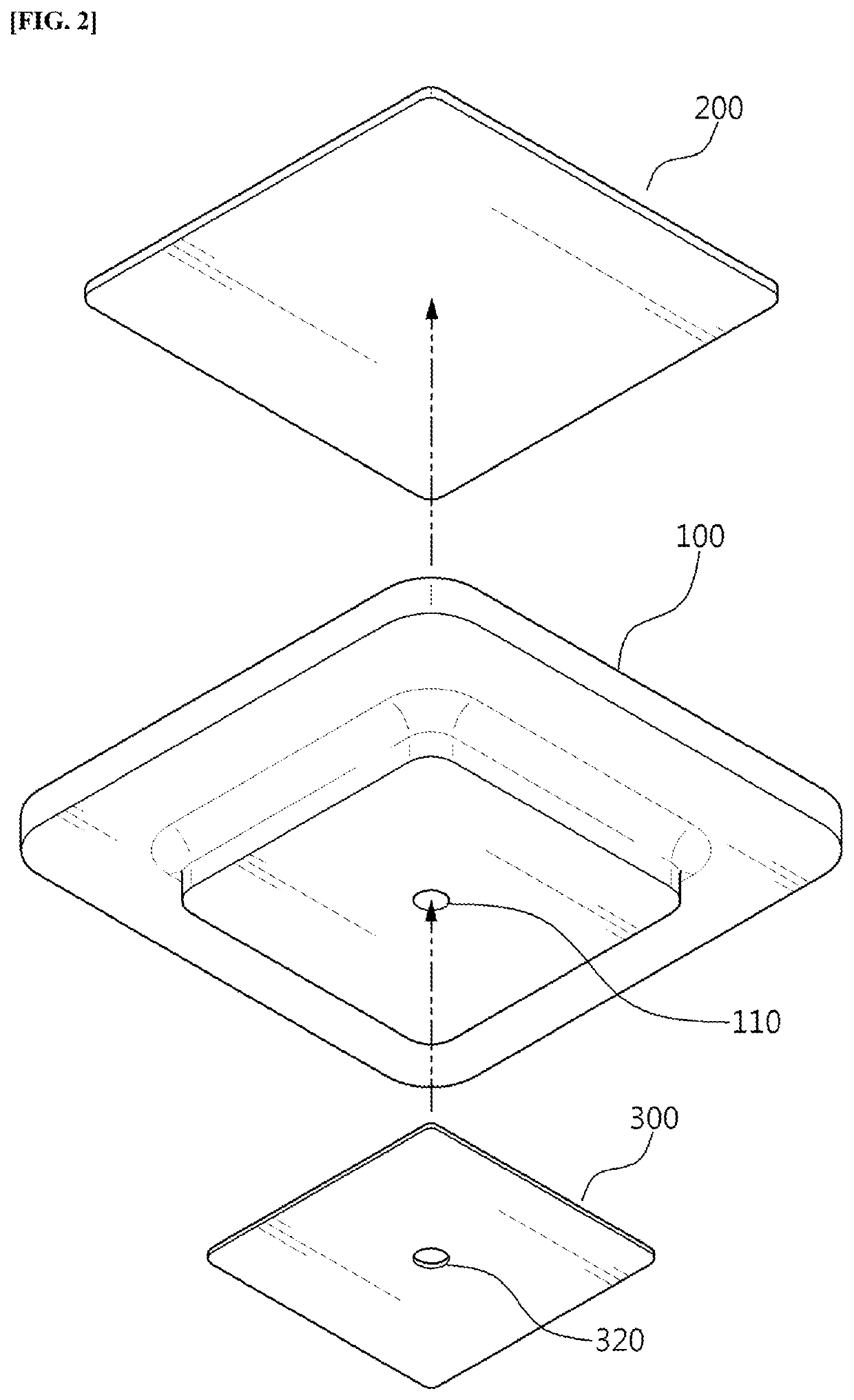
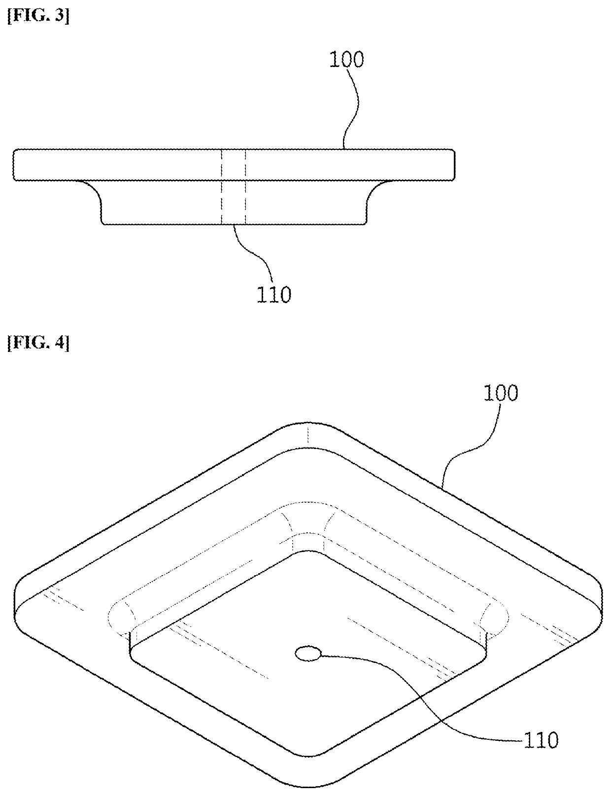
[0023]Referring to FIG. 2, a patch antenna according to an embodiment of the present disclosure is configured to include a dielectric layer 100, a radiation patch 200 bonded to the upper surface of the dielectric layer 100, and a lower patch 300 bonded to the lower surface of the d...


PUM

PropertyMeasurementUnit
frequenciesaaaaaaaaaa

Abstract

Disclosed is a patch antenna, which is formed so that the upper surface of a dielectric layer has a wider area than the lower surface thereof and is mounted on a printed circuit board to form an air gap, thus maximizing antenna performance while implementing lightweight. The disclosed patch antenna includes a dielectric layer, a radiation patch formed on the upper surface of the dielectric layer, and a lower patch formed on the lower surface of the dielectric layer; and the dielectric layer is formed so that an area of the upper surface is wider than an area of the lower surface to form an air gap between the printed circuit board and the dielectric layer.

Description

TECHNICAL FIELD[0001]The present disclosure relates to a patch antenna, and more particularly, to a patch antenna, which receives a signal in a frequency band of a GPS, a GNSS, SDARS, etc.BACKGROUND ART[0002]Generally, a patch antenna is installed in a vehicle, a drone, an information communication terminal, etc. to transmit and receive a signal in a frequency hand of a Global Positioning System (GPS), a Global Navigation Satellite System (GNSS), Satellite Digital Audio Radio Services (SDARS), etc.[0003]Referring to FIG. 1, a conventional patch antenna is composed of a dielectric layer 30 formed to have a predetermined thickness, an upper patch 10 in a planar shape that is stacked on one surface (upper surface) of the dielectric layer 30 and serves as an antenna, and a lower patch 20 stacked on the other surface (lower surface) of the dielectric layer 30.[0004]Herein, it is also referred to as a ceramic patch antenna because the dielectric layer 30 mainly uses a ceramic, which has g...

Claims


Application Information

Patent Timeline
Patent Type & Authority Applications(United States)
IPC IPC(8): H01Q9/04
CPCH01Q9/0414H01Q9/0407H01Q21/28H01Q1/38H01Q9/0442H01Q9/045
Inventor HWANG, CHULJEONG, IN-JOKIM, SANG-OOH, HYUN-WOOKOH, DONG-HWANLEE, WON-HEEPARK, TAE-BYUNGKANG, GI-CHOBAEK, KEUN-HO
Owner AMOTECH
Why Eureka
Try Eureka