Forming method of fin type field effect transistor

A technology of fin field effect transistors and fins, which is applied in the direction of electrical components, semiconductor/solid-state device manufacturing, circuits, etc., and can solve the problem of excessive contact resistance of fin field effect transistors and the inability to form metal contact layers on the side walls of fins, etc. problem, to achieve the effect of improved stability, reduced etching rate, and improved response speed

Active Publication Date: 2015-11-25
SEMICON MFG SOUTH CHINA CORP
View PDF7 Cites 3 Cited by
  • Summary
  • Abstract
  • Description
  • Claims
  • Application Information

AI Technical Summary

Problems solved by technology

[0006] The problem to be solved by the present invention is to avoid that the metal contact layer cannot be formed on the side wall of the fin due to the side wall formed on the side wall of the fin, and to avoid the excessive contact resistance of the fin field effect transistor.

Method used


Image

  • Forming method of fin type field effect transistor
  • Forming method of fin type field effect transistor
  • Forming method of fin type field effect transistor

Examples


Embodiment Construction

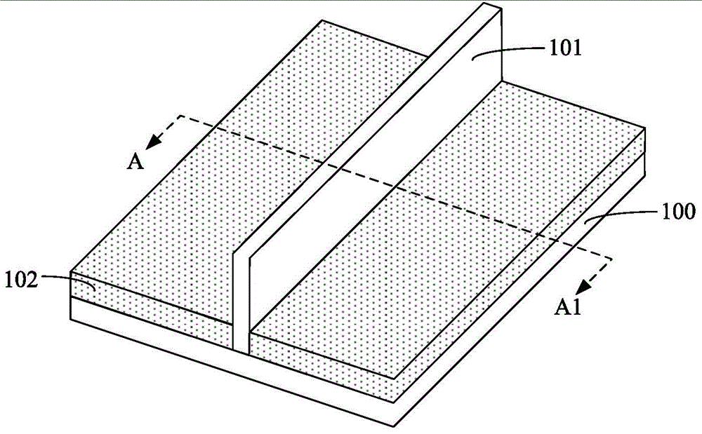
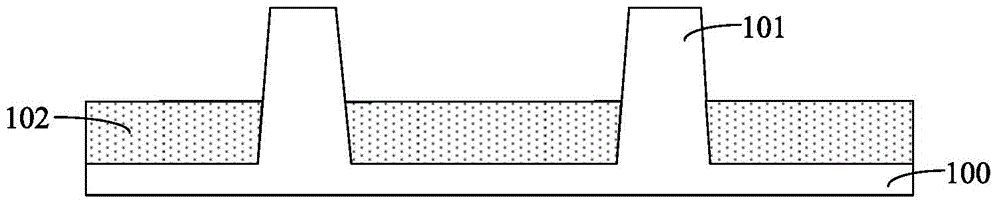
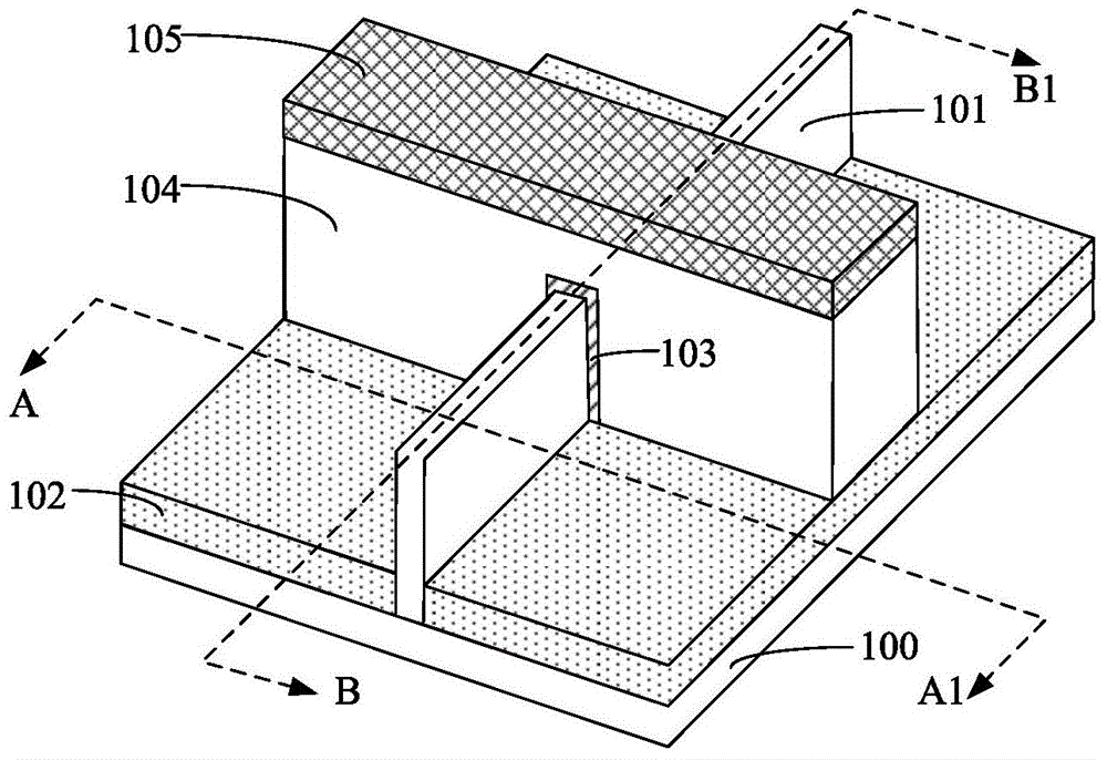
[0032] It can be seen from the background technology that the electrical performance of the FinFET provided by the prior art needs to be improved. For example, the contact resistance of the FinFET is relatively large, the response rate of the FinFET is low, and the FinFET Weak ability to electrically connect with other devices.

[0033] After research, it is found that the reason for the large contact resistance of the FinFET and the weak ability to electrically connect with other devices is: in order to reduce the contact resistance of the FinFET and make the FinFET electrically connected to other devices. Connection, usually form a metal contact layer in the source and drain regions of the FinFET, for example, the material of the metal contact layer is NiSi, in order to reduce the contact resistance of the FinFET and improve the response speed of the FinFET , and the fin field effect transistor can also be electrically connected to other devices through the metal contact lay...


PUM


Abstract

A forming method of a fin type field effect transistor includes the steps: providing a substrate, wherein a plurality of separate fins are formed on the surface of the substrate, and a grid electrode structure crossing the fins is formed on the surface of the substrate; forming spacer films on the sidewall of the grid electrode structure, the top surface of the grid electrode structure, sidewalls of the fins, top surfaces of the fins and the surface of the substrate; conducting back etching on the spacer films through an anisotropic etching process, removing the spacer films on the surface of the substrate, the top surface of the grid electrode structure and the top surfaces of the fins, forming a first spacer on the sidewall of the grid electrode structure, and forming second spacers on the sidewalls of the fins; carrying out doping processing on the first spacer, and reducing the etching rate of the isotropic etching process for the first spacer; etching and removing the second spacers through an isotropic etching process, making the sidewalls of the fins exposed, and keeping the first spacer of the sidewall of the grid electrode structure; forming doped regions inside the fins at the two sides of the first spacer; and forming metal contact layers on the sidewalls and the top surfaces of the fins. The contact resistance of a fin type field effect transistor is reduced, and the response speed of the fin type field effect transistor is increased.

Description

technical field [0001] The invention relates to the technology in the field of semiconductor manufacturing, in particular to a method for forming a fin field effect transistor. Background technique [0002] With the continuous development of semiconductor process technology, the development trend of semiconductor process nodes following Moore's Law continues to decrease. In order to adapt to the reduction of process nodes, the channel length of MOSFET field effect transistors has to be continuously shortened. The shortening of the channel length has the advantages of increasing the die density of the chip and increasing the switching speed of the MOSFET field effect tube. [0003] However, as the channel length of the device is shortened, the distance between the source and the drain of the device is also shortened, so that the control ability of the gate to the channel becomes worse, and the gate voltage pinches off (pinchoff) the channel. The difficulty is also increasin...

Claims


Application Information

Patent Timeline
Patent Type & Authority Applications(China)
IPC IPC(8): H01L21/336H01L21/3065
Inventor 何有丰
Owner SEMICON MFG SOUTH CHINA CORP
Why Eureka
Try Eureka