

Low etching photoresist cleaning agent
A cleaning agent and etching technology, applied in the field of cleaning agents, can solve the problems of poor cleaning effect, strong corrosion of substrates, low etching of wafer substrates, etc., and achieve good application prospects
Inactive Publication Date: 2008-10-15
ANJI MICROELECTRONICS (SHANGHAI) CO LTD
View PDF5 Cites 22 Cited by
- Summary
- Abstract
- Description
- Claims
- Application Information
AI Technical Summary
Problems solved by technology
[0008] The purpose of the present invention is to solve the problem of poor cleaning effect of existing cleaning agents or strong corrosion on substrates in the photoresist cleaning process, and to provide a cleaning agent with high cleaning effect and low impact on wafer substrates. Etching Photoresist Cleaner
Method used
View moreImage
Smart ImageViewing Examples

Examples
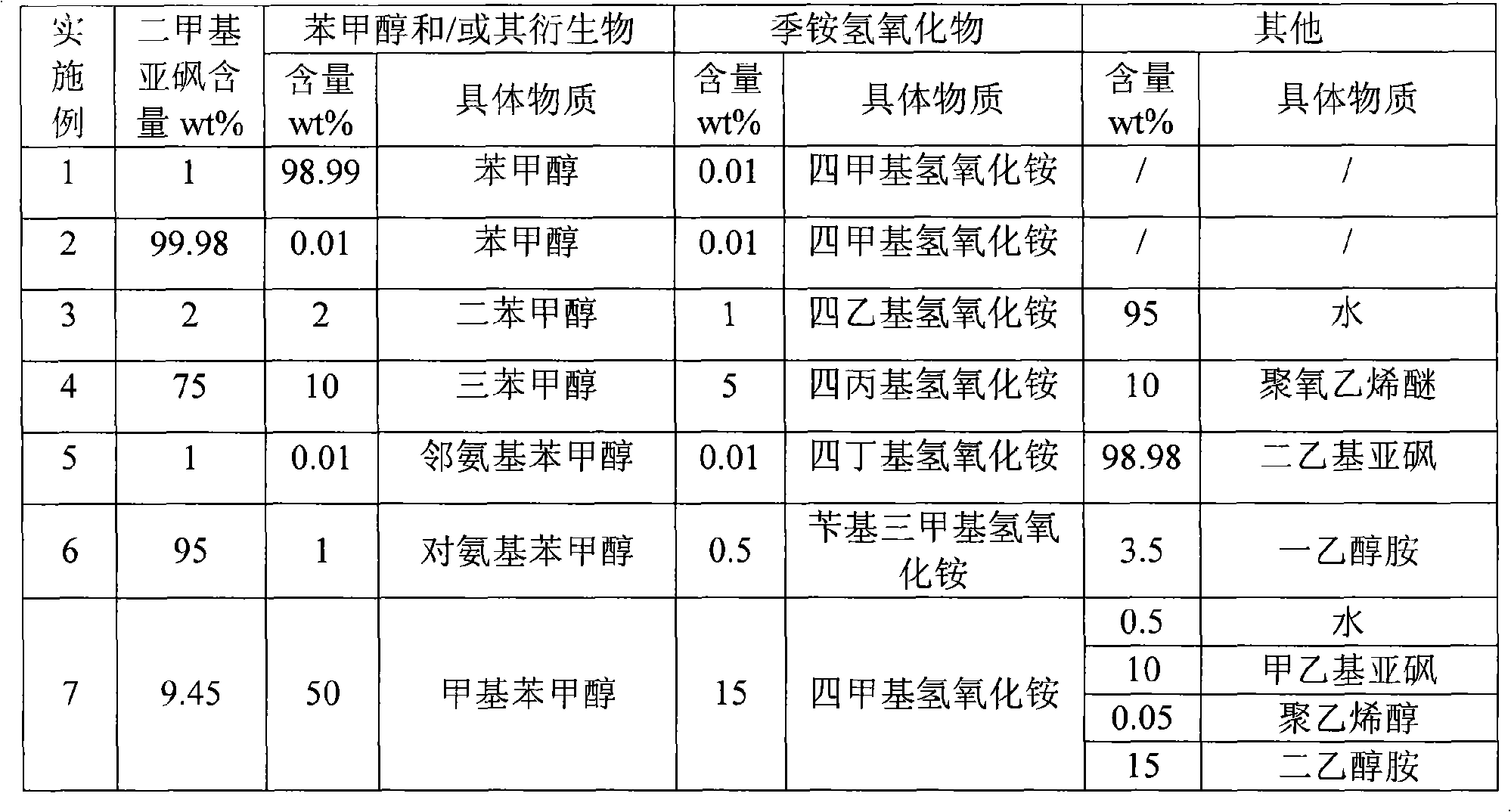
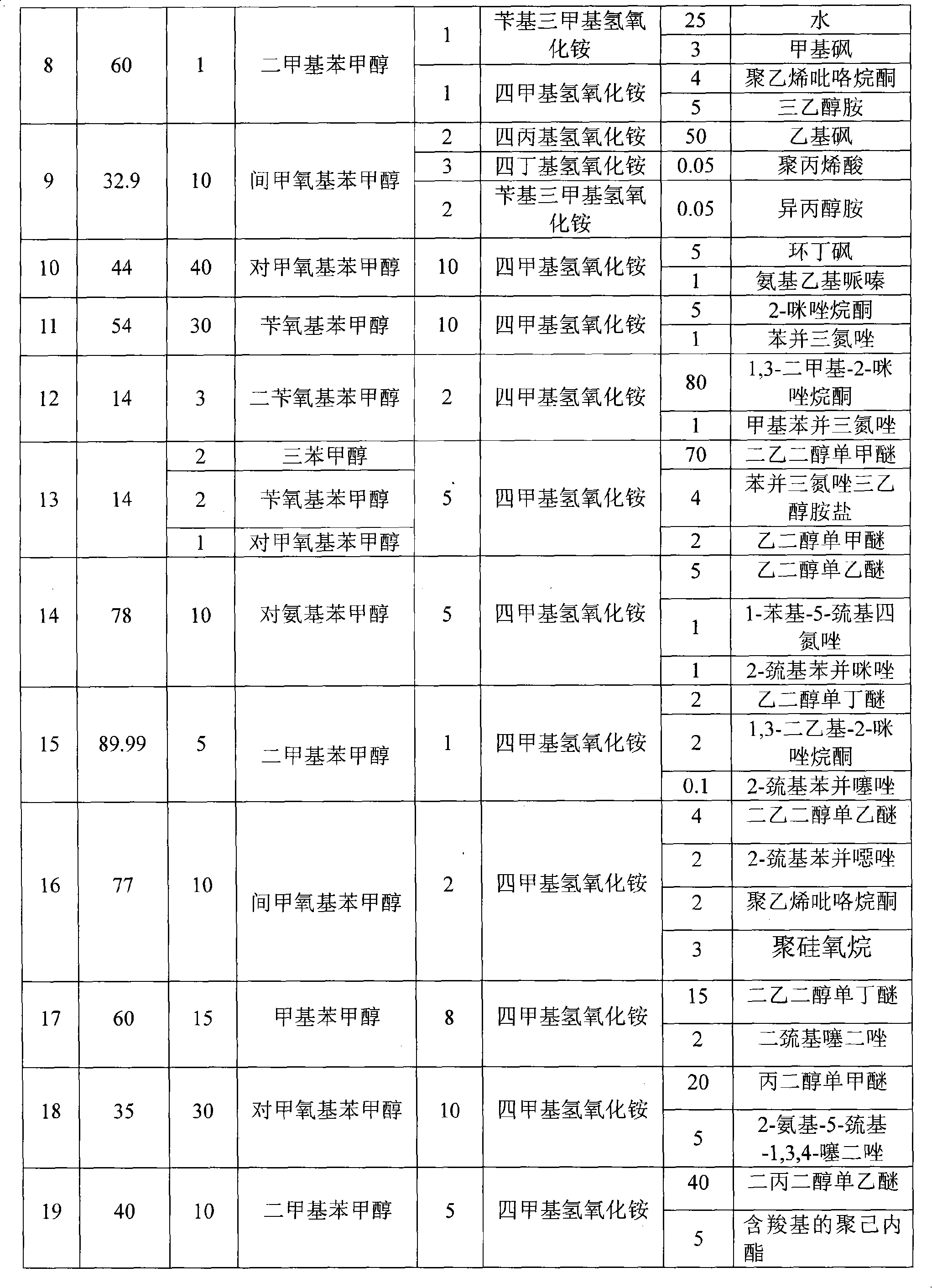
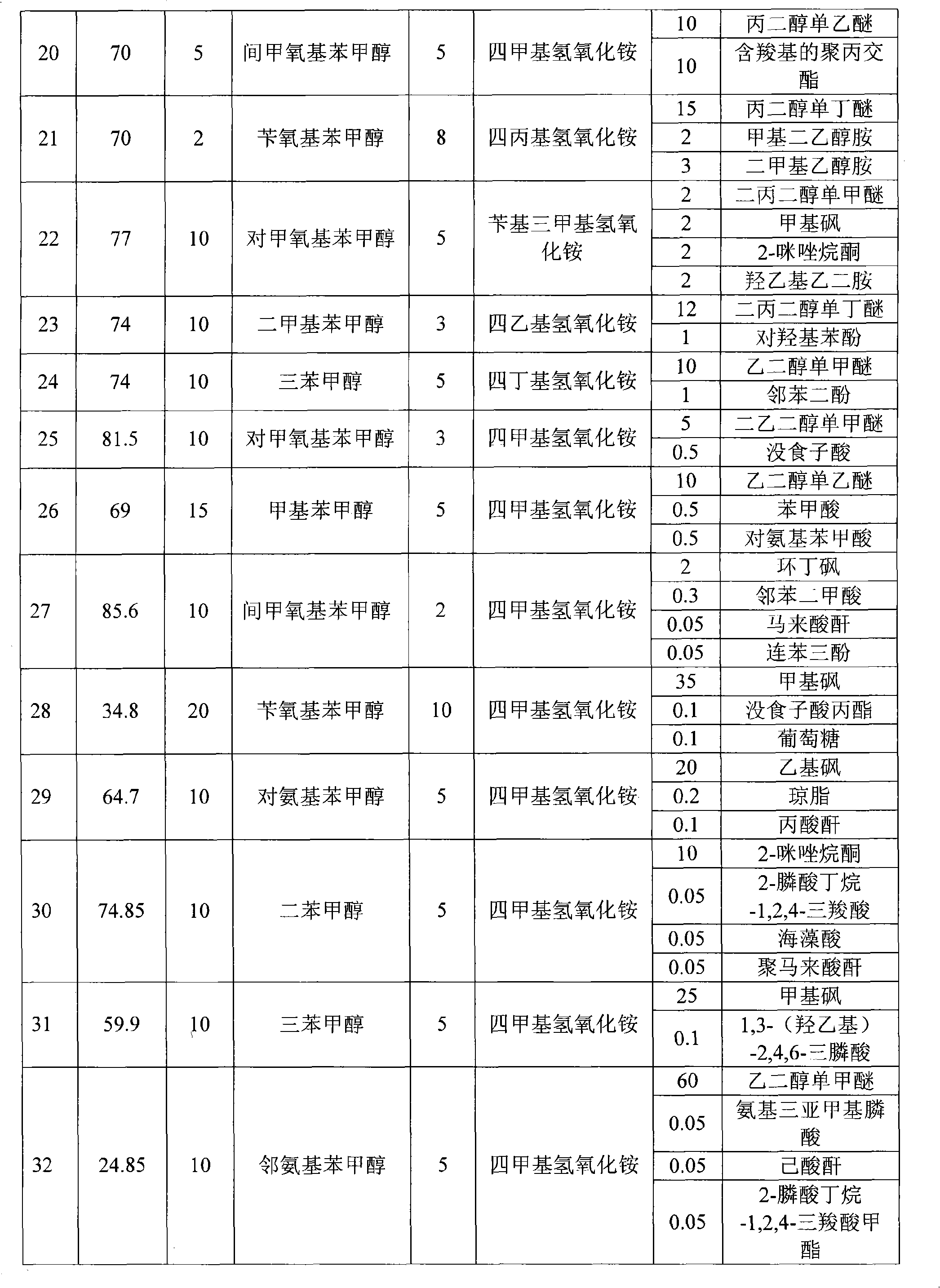
Embodiment 1~32
[0022] Table 1 shows Examples 1 to 32 of the low-etching photoresist cleaning agent of the present invention. According to the formula given in the table, the components can be used simply by mixing them evenly.
[0023] Table 1 Low Etching Photoresist Examples 1-32
[0024]
[0025]
[0026]
Login to View More PUM
 Abstract
The invention discloses a low etching photoresist cleaning agent, comprising benzyl alcohol and / or ramification of the benzyl alcohol, quaternary ammonium hydroxide and dimethyl sulfoxide. The cleaning agent of the invention can be used for removing photoresist (light resistance) and other residues on metals, metal alloys or dielectric substrates, has low etching speed on metals such as SiO2, copper, etc. and low-k material, and has excellent application prospect in micro-electron fields such as semiconductor wafer cleaning, etc.
Description
technical field [0001] The invention relates to a cleaning agent in a semiconductor manufacturing process, in particular to a photoresist cleaning solution. Background technique [0002] In the usual semiconductor manufacturing process, a photoresist mask is formed on the surface of metals such as silicon dioxide, copper, and low-k materials, and pattern transfer is performed by wet or dry etching after exposure. Low temperature and fast cleaning process is an important direction for the development of semiconductor wafer manufacturing process. In the process of chemically cleaning the photoresist on the semiconductor wafer, the cleaning agent often causes serious corrosion to the wafer substrate, especially the corrosion of the metal substrate, which often leads to a significant decrease in wafer yield. The photoresist cleaning agents disclosed in the prior art more or less have the problem of poor cleaning effect or corrosion of the wafer substrate. [0003] Patent docum...
Claims
Login to View More Application Information
Patent Timeline
 IPC IPC(8): G03F7/42
CPCG03F7/425C11D7/261C11D7/3209C11D7/34C11D7/5009G03F7/426
Inventor史永涛彭洪修刘兵曾浩
OwnerANJI MICROELECTRONICS (SHANGHAI) CO LTD