Novel method to deposit carbon doped SiO2 films with improved film quality

a carbon doped sio2 film and film quality technology, applied in the field of fabrication integrated circuits and other electronic devices, can solve the problems of reducing device performance, affecting the quality of carbon doped sio2 films, and the cost of deposited low k dielectric layers, so as to reduce the frequency of preventative maintenance cleaning operations in the cvd chamber, the effect of improving the deposition ra

Inactive Publication Date: 2005-06-09
TAIWAN SEMICON MFG CO LTD
View PDF5 Cites 21 Cited by
  • Summary
  • Abstract
  • Description
  • Claims
  • Application Information

AI Technical Summary

Benefits of technology

[0009] An objective of the present invention is to provide a method of depositing a carbon doped SiO2 layer such as a Black Diamond film that provides a higher deposition rate than conventional CVD methods.
[0010] A further objective of the present invention is to provide a method of depositing a carbon doped SiO2 layer which maintains good film thickness uniformity for a larger number of wafers successively processed in a CVD chamber so that the frequency of preventative maintenance cleaning operations in the CVD chamber may be reduced.
[0011] A still further objective of the present invention is to provide a method of depositing a carbon doped SiO2 layer that has increased hardness and a higher value for tensile strength (Young's modulus).
[0012] Yet another objective of the present invention is to provide a method of depositing a carbon doped SiO2 layer that has better thermal and chemical stability including a higher resistance to O2 ashing and a lower etch rate in a fluorocarbon based plasma.
[0013] These objectives are achieved by providing a substrate and a CVD process chamber. Once the substrate is loaded into the CVD chamber, the chamber is heated to an appropriate temperature and the chamber pressure is reduced to an acceptable level. A low k dielectric layer comprising carbon doped SiO2 is deposited on the substrate by flowing oxygen, an inert gas which is preferably argon, and an organosilane that is preferably trimethylsilane at a preferred ratio of 1:1.5:6 into the chamber while a plasma is generated. Argon is flowed into the chamber during the PECVD process at a sufficient rate to increase the deposition rate of the carbon doped SiO2 film and to provide a bombardment effect that densifies, hardens, and improves the tensile strength of the film. High Ar flow rates that increase the dielectric constant of the deposited film and low Ar flow rates that lead to a higher than desired porosity in the film are avoided. The carbon doped SiO2 film is deposited at a high enough temperature so that a post-deposition anneal is not required. At this point the substrate may be removed or another dielectric layer such as a cap layer or anti-reflective coating (ARC) may be deposited on the carbon doped SiO2 layer in the CVD process chamber.
[0014] In one application, the low k dielectric layer is deposited on an etch stop layer which has been formed on a substrate in a single or dual damascene scheme. Optionally, a cap layer or an ARC is deposited on the low k dielectric layer. A via opening is formed in the low k dielectric layer and a trench is fabricated above the via by a conventional sequence of patterning and etching steps. After an etch step removes the etch stop layer at the bottom of the via, a conformal diffusion barrier layer is deposited in the via and trench followed by deposition of a metal layer to fill the via and trench. A planarization step completes the damascene scheme. The improved physical and mechanical properties of the low k dielectric layer enable a lower leakage current and higher breakdown voltage in the resulting metal interconnect.

Problems solved by technology

Unfortunately, a low k dielectric layer is often porous and may require a treatment to densify the layer in order to prevent water absorption that will increase the effective dielectric constant.
Furthermore, the hardness and tensile strength of a low k dielectric layer is a concern since a CMP planarization step can easily cause scratches, peeling, or cracking in a low k dielectric layer that will degrade device performance.
Another important issue is the cost associated with depositing a low k dielectric layer.
Organosilicon precursors are more expensive than silane which is used to form SiO2.
Moreover, the deposition rate of a Black Diamond film is only about half that of SiO2 formed from SiH4 and O2 and the lower deposition rate slows throughput in the manufacturing line.
As the deposition process is repeated hundreds of times and the buildup on the chamber walls increases, the low k dielectric material on the walls appears to adversely influence the film uniformity of the low k dielectric layer deposited on a wafer.
At this point, the process chamber must be taken out of service for cleaning purposes which decreases throughput.
However, neither reference provides process conditions for the low k dielectric layer deposition.
However, the prior art does not teach the importance of the relationship between the Ar flow rate and the O2 and organosilicon flow rates in improving film quality and increasing the deposition rate.

Method used


Image

  • Novel method to deposit carbon doped SiO2 films with improved film quality
  • Novel method to deposit carbon doped SiO2 films with improved film quality
  • Novel method to deposit carbon doped SiO2 films with improved film quality

Examples


Embodiment Construction

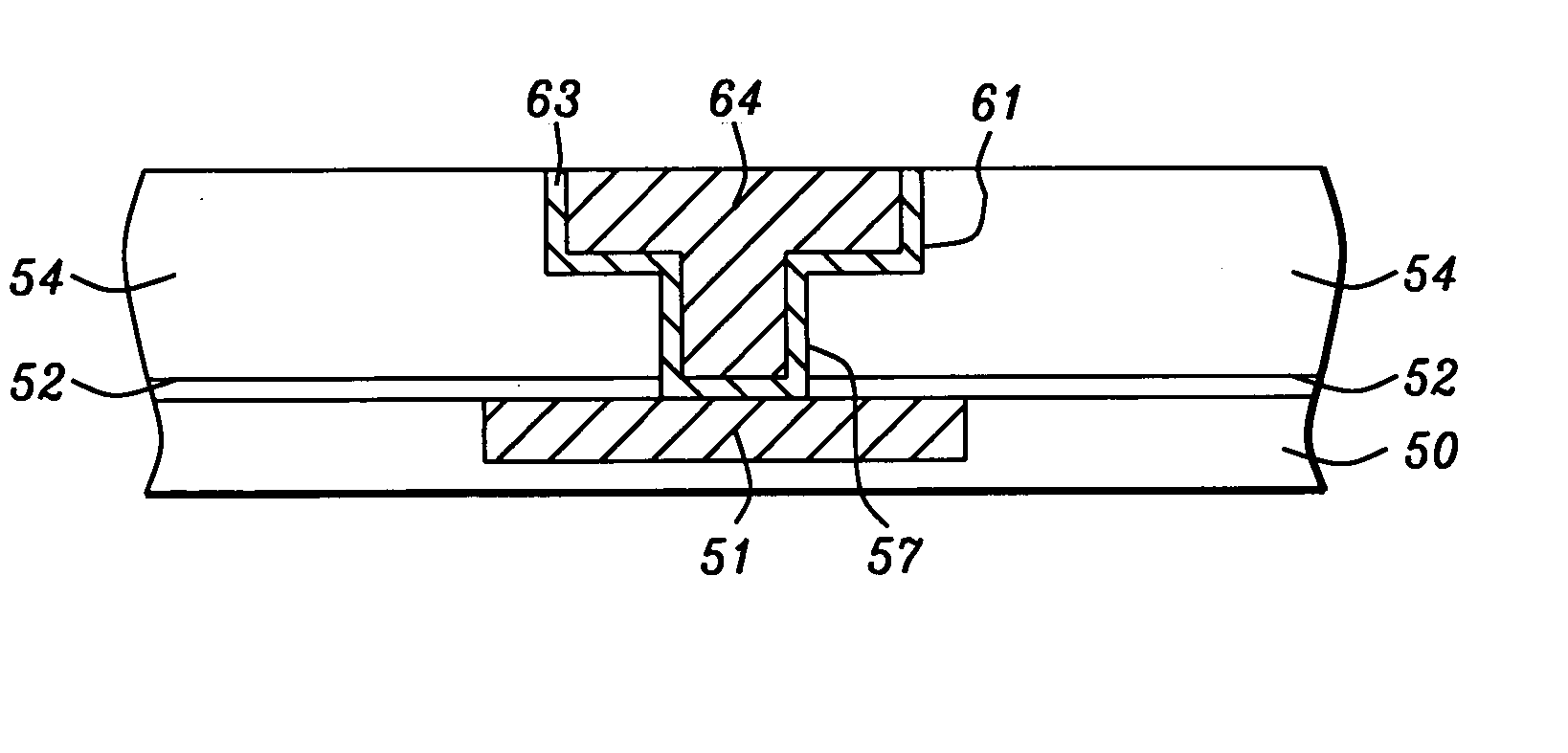
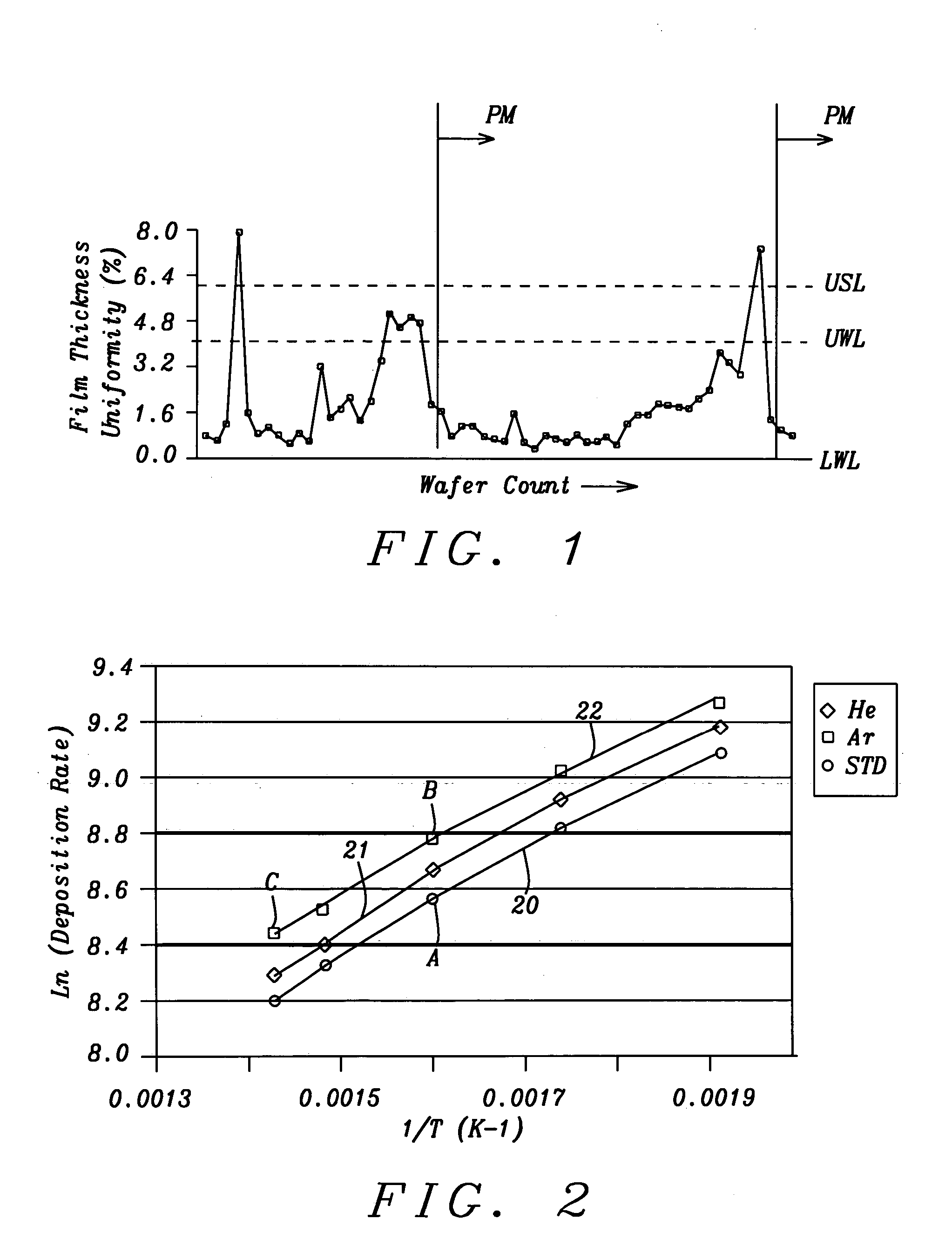
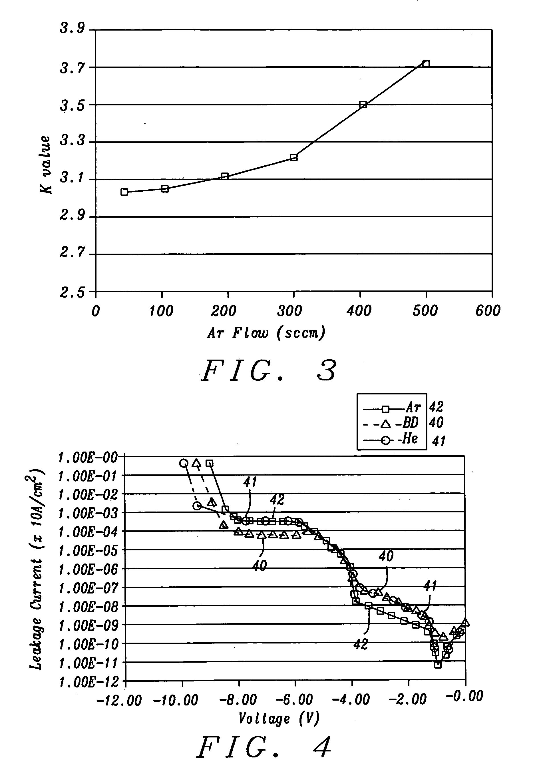
[0022] The invention is a method of depositing a carbon doped SiO2 film as a low k dielectric layer to insulate metal interconnects in a semiconductor device. The drawings are provided by way of example and are not intended to limit the scope of the invention. Moreover, the figures are not necessarily drawn to scale and the relative size of various elements may be different than found in an actual device. Although FIGS. 5-9 depict the use of an interlevel dielectric layer (ILD) in a damascene scheme for fabricating a metal interconnect, those skilled in the art will appreciate that a carbon doped SiO2 layer may also be deposited according to a method of the present invention in a gap fill operation (not shown) to form an intermetal dielectric (IMD) layer between metal lines formed on a substrate.

[0023] It is understood that the deposition method of the present invention may be performed in any chemical vapor deposition (CVD) process chamber to form a carbon doped SiO2 layer and tha...


PUM

PropertyMeasurementUnit
pressureaaaaaaaaaa
pressureaaaaaaaaaa
temperatureaaaaaaaaaa

Abstract

A method is disclosed for depositing a Black Diamond layer in a CVD chamber. Trimethylsilane, O2, and Ar are flowed into the chamber at 300° C. to 400° C. with an O2:Ar:trimethylsilane flow rate ratio that is preferably 1:1.5:6. The resulting low k dielectric layer is formed with a higher deposition rate than when Ar is omitted and has a k value of about 3 that increases only slightly in O2 plasma. A higher density, hardness, and tensile strength are achieved in the Black Diamond layer when Ar is included in the deposition process. The addition of Ar in the deposition maintains film thickness uniformity below 2% for a longer period so that PM cleaning operations are less frequent and affords a lower fluorocarbon plasma etch rate to enable improved trench depth control in a damascene scheme. A lower leakage current and higher breakdown voltage in achieved in the resulting metal interconnect.

Description

FIELD OF THE INVENTION [0001] The invention relates to the field of fabricating integrated circuits and other electronic devices and in particular to a method of improving the properties of a carbon doped SiO2 low k dielectric layer that is deposited by a plasma enhanced chemical vapor deposition (PECVD) method. BACKGROUND OF THE INVENTION [0002] The fabrication of a high performance electronics device involves the formation of metal interconnects as electrical pathways and the deposition of one or more dielectric layers to insulate one interconnect from another. Metal interconnects are typically trenches, vias, or contact holes that are filled with a metal such as copper. One popular method for forming an interconnect is a damascene process in which an opening is etched in a dielectric layer, a metal is deposited in the opening, and a planarization step such as a chemical mechanical polish (CMP) step is used to make the metal coplanar with the top of the dielectric layer. [0003] A ...

Claims


Application Information

Patent Timeline
Patent Type & Authority Applications(United States)
IPC IPC(8): C23C16/40H01L21/316H01L21/768
CPCC23C16/401H01L21/02126H01L21/02211H01L21/02274H01L21/76819H01L21/02362H01L21/31633H01L21/76801H01L21/76807H01L21/02304
Inventor CHENG, YI-LUNGLIU, REN-HAURLIU, CHENG-HSIUNGWANG, YING-LANGLIN, HWAY-CHICHIU, CHIEN-MING
Owner TAIWAN SEMICON MFG CO LTD
Why Eureka
Try Eureka