

Optical filter, and imaging device comprising same
a technology of optical filters and imaging devices, applied in the direction of camera filters, instruments, cameras, etc., can solve problems such as image distortion, and achieve the effect of preventing a shift in the transmission spectrum and hindering the transmittance in the visible region
- Summary
- Abstract
- Description
- Claims
- Application Information
AI Technical Summary
Benefits of technology
Problems solved by technology
Method used
Image

Examples
example 1
Preparative Example 1
[0067]TiO2 and SiO2 were alternately stacked on one surface of a glass substrate using an E-beam evaporator to form a near-infrared reflection layer.
[0068]Separately, a light absorbing agent which is commercially available and has an absorption maximum of 670 nm, a cyclic olefin-based resin as a binder resin source, and toluene (commercially available from Sigma Aldrich) were mixed and then stirred for at least a day using a magnetic stirrer to prepare a near-infrared absorbing solution.
[0069]Next, the prepared near-infrared absorbing solution was spin-coated onto an opposite surface of the glass substrate on which the near-infrared reflection layer was formed to form a light absorption layer.
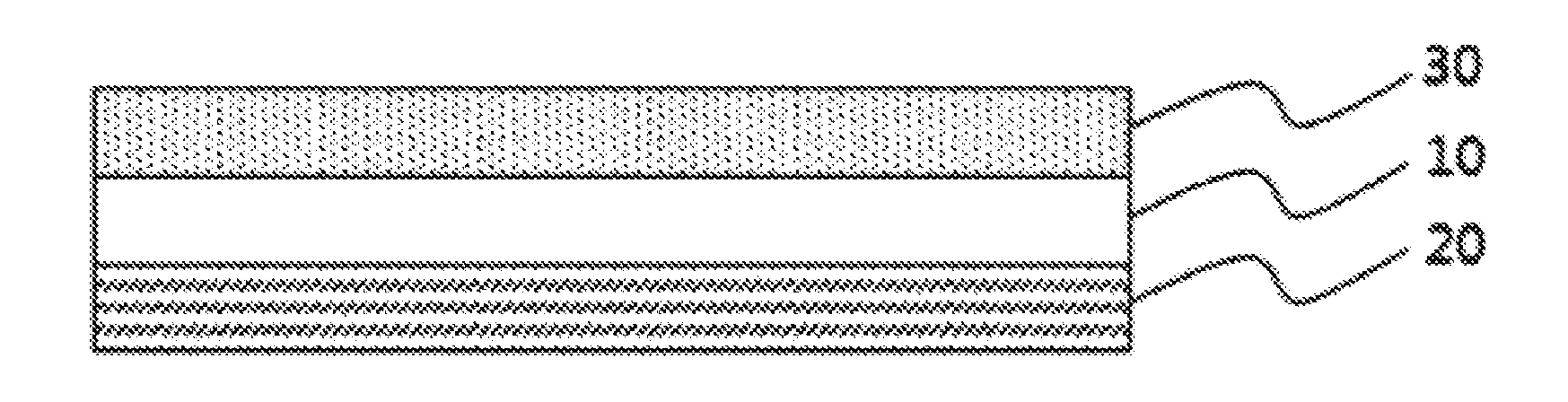
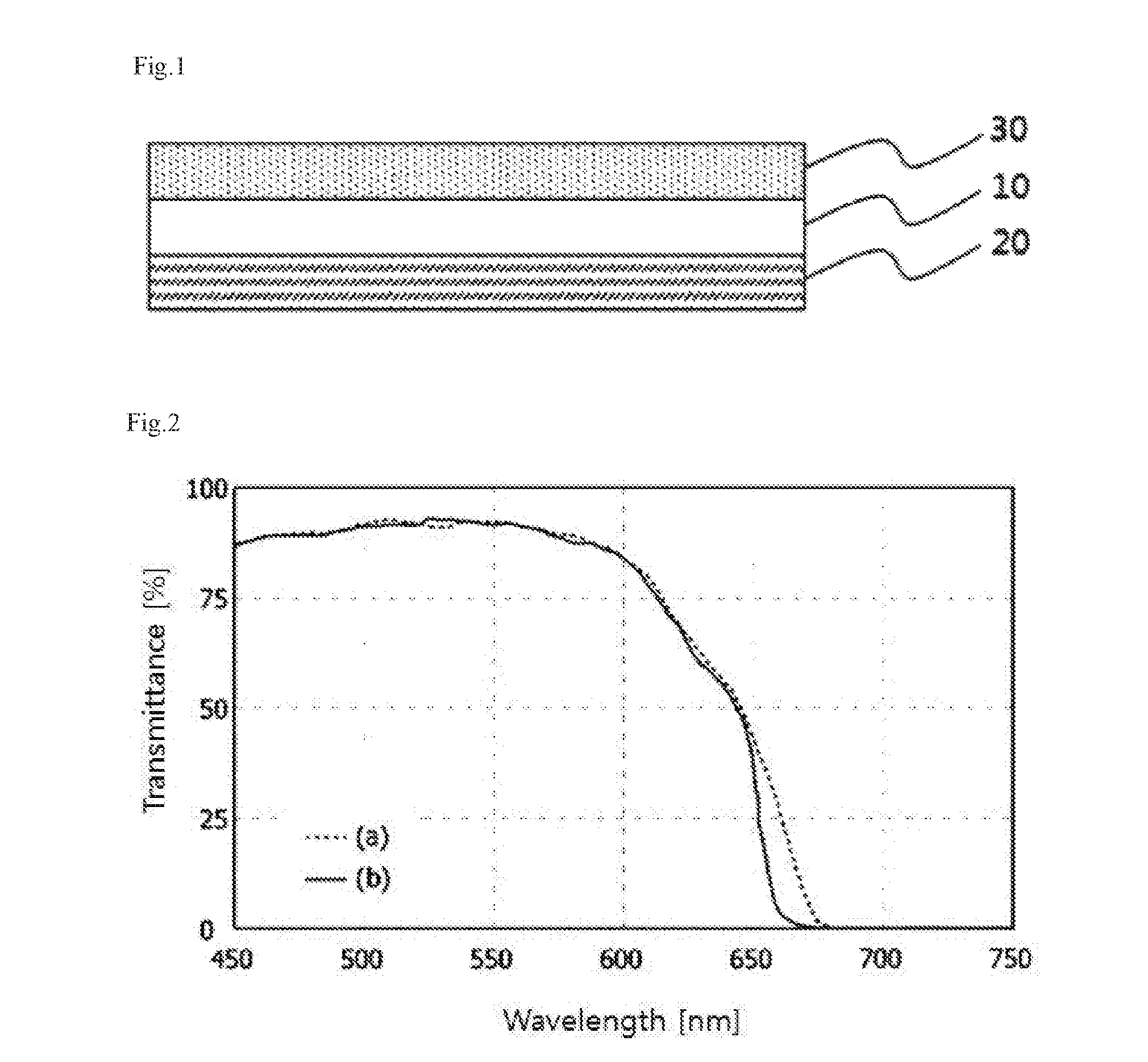
[0070]The optical filter according to one exemplary embodiment of the present invention was manufactured using the above-described method. A stacked structure of the manufactured optical filter is shown in FIG. 1. Referring to FIG. 1, a near-infrared reflection layer 20 is ...
example 2
Preparative Example 2
[0072]An optical filter was manufactured in the same manner as in Preparative Example 1, except that a light absorbing agent which was commercially available and had an absorption maximum of 700 nm was used instead.
experimental example 1
[0073]The optical filters manufactured in Preparative Examples 1 and 2 were measured for ΔE*.
[0074]Specifically, the color coordinates L*, a* and b* of the light passing through each of the optical filters when white light was irradiated on the manufactured absorption filter in the vertical direction (an angle of incidence of 0°) and irradiated at an angle of 30° with respect to the vertical direction of the absorption filter were measured using spectrophotometer Lambda 35 commercially available from Perkin Elmer, and the ΔE* was then calculated.
[0075]Also, W1, W2 and W3 were measured to calculate a W2−W1 value and a W1−(W2−W3 / 2) value. The W2−W1 value as shown in Mathematical Formula 2, and the W1−(W2−W3 / 2) value as shown in Mathematical Formula 3 were measured.
[0076]In this case, the wavelength W1 at which the near-infrared reflection layer had a transmittance of 50% was controlled to be within 650 nm to 750 nm range by varying the alternate stacking number of TiO2 and SiO2 used t...
PUM
 Abstract
Description
Claims
Application Information