Thin Film Transistor and Method of Fabricating the Same, Array Substrate and Method of Fabricating the Same, and Display Device

a thin film transistor and array substrate technology, applied in the field of display technology, can solve the problems of low process yield, long process time, high fabrication cost of array substrate, etc., and achieve the effects of low manufacturing cost, simple manufacturing process and high fabricating cos

Active Publication Date: 2016-09-01
BOE TECH GRP CO LTD
View PDF3 Cites 10 Cited by
  • Summary
  • Abstract
  • Description
  • Claims
  • Application Information

AI Technical Summary

Benefits of technology

[0013]To solve the technical problem of high fabricating cost of the low-temperature polysilicon array substrate in the prior art, the present invention provides a low-temperature polysilicon thin film transistor and a method of fabricating the s

Problems solved by technology

As can be seen from above, at least six to seven photolithography processes are required to form the structure of the low-temperature polysilicon array substrate shown in FIG. 1, resulting in long process time and low process yield, so that fabrication cost of the array substrate is high.
Further, the inventor finds that, since excess silicon atoms migrate to port

Method used


Image

  • Thin Film Transistor and Method of Fabricating the Same, Array Substrate and Method of Fabricating the Same, and Display Device
  • Thin Film Transistor and Method of Fabricating the Same, Array Substrate and Method of Fabricating the Same, and Display Device
  • Thin Film Transistor and Method of Fabricating the Same, Array Substrate and Method of Fabricating the Same, and Display Device

Examples


first embodiment

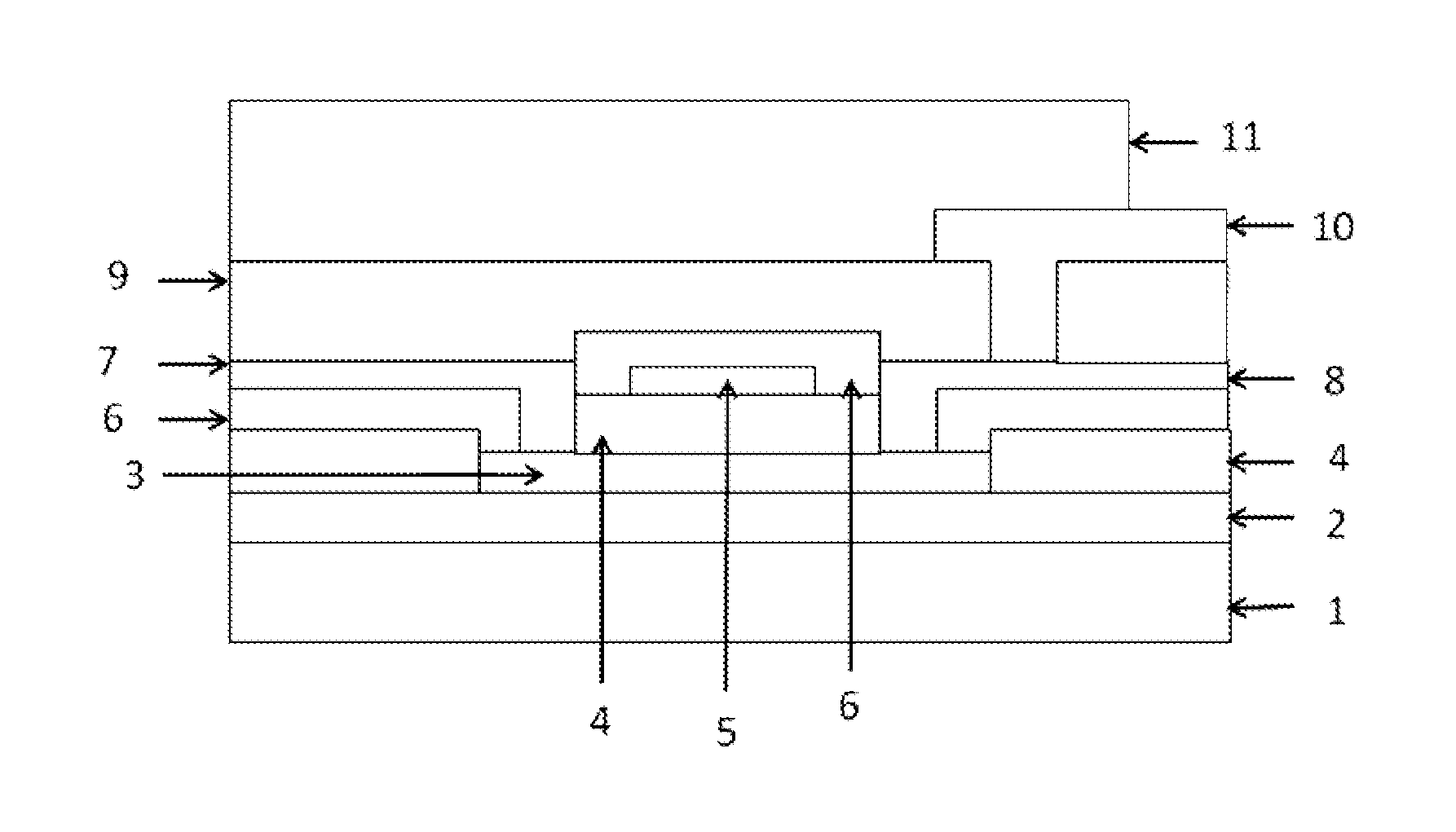
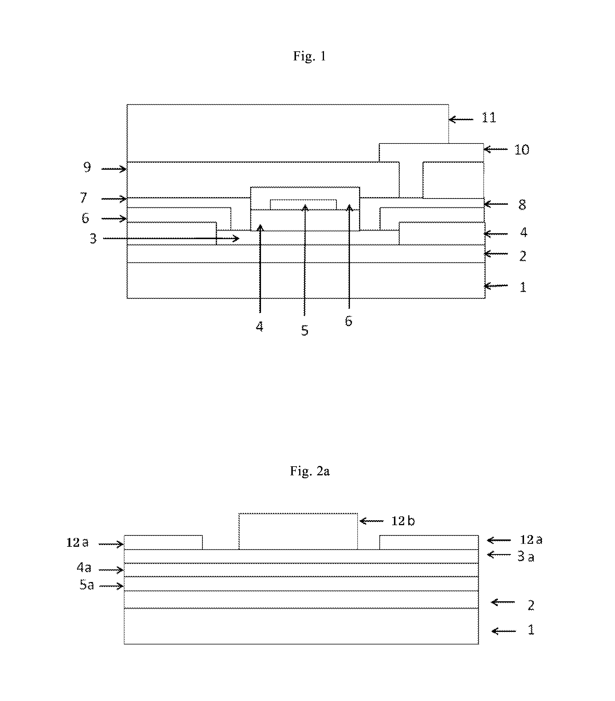
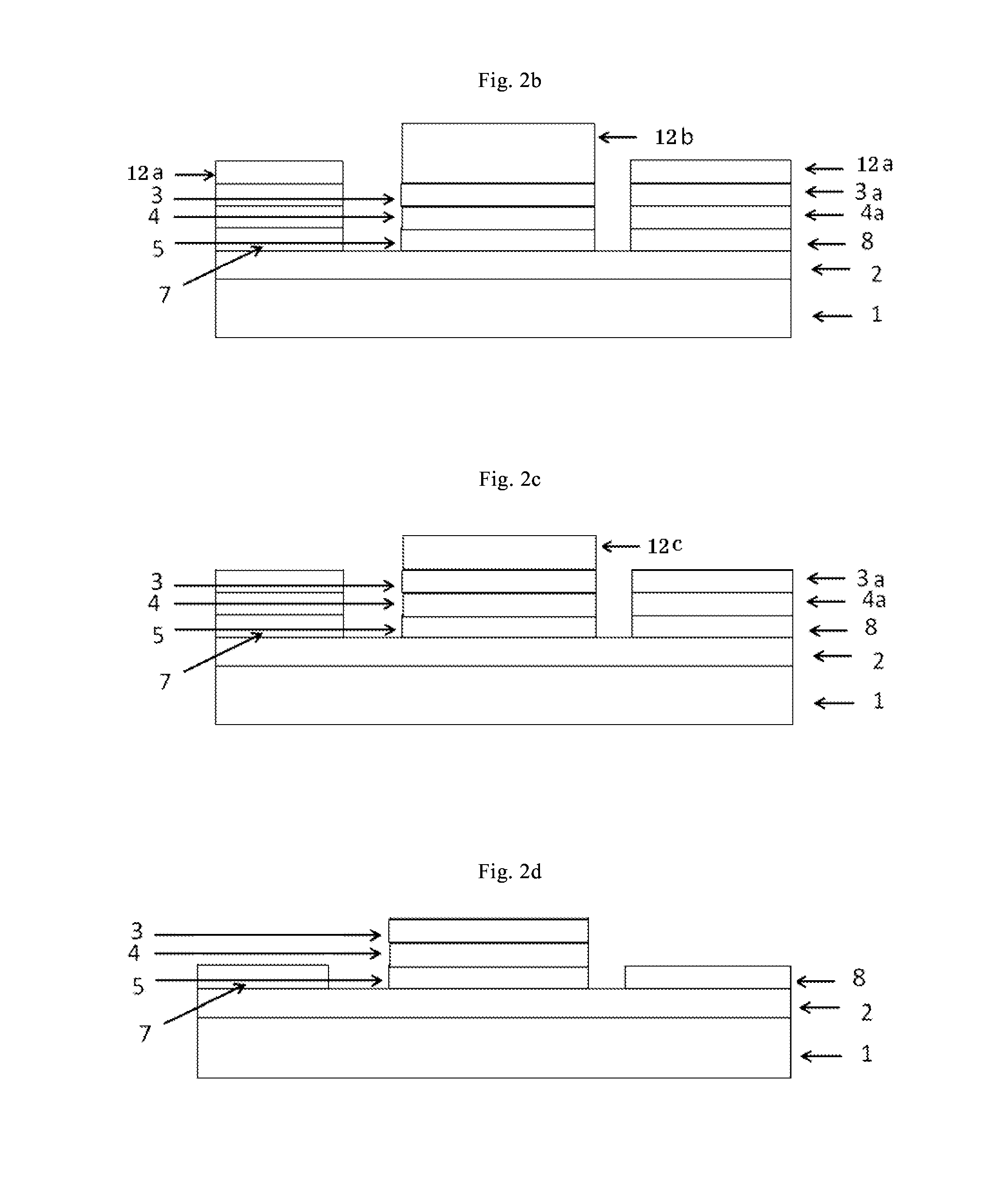
[0040]Referring to FIGS. 2a through 2i, the embodiment of the present invention provides a low-temperature polysilicon thin film transistor and a method of fabricating the same. Referring to FIG. 2i, the thin film transistor comprises a gate 5, a source 7, a drain 8, a gate insulation layer 4, an active layer 3, a passivation layer 6, a first electrode connection line 15a and a second electrode connection line 15b. In the thin film transistor, the gate 5, the source 7 and the drain 8 are provided in the same layer and comprise the same material; the gate insulation layer 4 is provided on the gate 5, the active layer 3 is provided on the gate insulation layer 4, a pattern of the gate insulation layer 4, a pattern of the gate 5 and a pattern of the active layer 3 coincide with each other; the passivation layer 6 covers the source 7, the drain 8 and the active layer 3, and the passivation layer 6 has a first via hole 14a corresponding to a position of the source 7, a second via hole 14...

second embodiment

[0057]This embodiment provides an array substrate and a method of fabricating the same, and the array substrate comprises the thin film transistor described in the first embodiment.

[0058]As shown in FIG. 2j, the array substrate of the embodiment further comprises a pixel electrode 10 and a pixel defining layer 11. The pixel electrode 10, the first electrode connection line 15a and the second electrode connection line 15b are provided in the same layer and comprise the same material. Therefore, the pixel electrode 10, the first electrode connection line 15a and the second electrode connection line 15b of the embodiment may be formed by one patterning process.

[0059]As shown in FIGS. 3 and 4, as one case of the embodiment, the array substrate further comprises a plurality of gate lines and a plurality of data lines 17 intersecting with each other and insulated from each other, each gate line comprises a plurality of gate line strips 16a and a third electrode connection line 15c connect...

third embodiment

[0081]This embodiment provides a display device that comprises the array substrate in the second embodiment.

[0082]The display device may be any product or component with a display function, such as mobile phone, tablet computer, TV set, display, notebook computer, digital photo frame, navigator, etc.

[0083]Of course, the display device of the embodiment may further comprise other conventional structure such as display driving unit, etc.


PUM


Abstract

The present invention provides a thin film transistor and a method of fabricating the same, an array substrate and a method of fabricating the same, and a display device. The thin film transistor comprises a gate, a source, a drain, a gate insulation layer, an active layer, a passivation layer, a first electrode connection line and a second electrode connection line. The gate, the source and the drain are provided in the same layer and comprise the same material. The gate insulation layer is provided above the gate, the active layer is provided above the gate insulation layer, and a pattern of the gate insulation layer, a pattern of the gate and a pattern of the active layer coincide with each other. The passivation layer covers the source, the drain and the active layer, and the passivation layer has a first via hole corresponding to a position of the source, a second via hole corresponding to a position of the drain, and a third via hole and a fourth via hole corresponding to a position of the active layer provided therein. The first electrode connection line connects the source with the active layer through the first via hole and the third via hole, and the second electrode connection line connects the drain with the active layer through the second via hole and the fourth via hole.

Description

FIELD OF THE INVENTION[0001]The present invention relates to the field of display technology, and particularly relates to a low-temperature polysilicon thin film transistor and a method of fabricating the same, an array substrate and a method of fabricating the same, and a display device.BACKGROUND OF THE INVENTION[0002]An organic light emitting diode display has advantages of high response speed, light weight, flexible and wide viewing angle with respect to a liquid crystal display. An active matrix organic light emitting diode (AMOLED) has advantages of low driving current and low power consumption, and is suitable for high-resolution display. The architecture of the active matrix organic light emitting diode may be driven by using amorphous silicon, polysilicon, oxide semiconductor or organic thin film transistor, since a carrier mobility and a driving current of amorphous silicon or organic thin film transistor are small, a voltage required for driving high-luminance organic lig...

Claims


Application Information

Patent Timeline
IPC IPC(8): H01L27/12H01L29/49H01L29/786
CPCH01L27/1244H01L27/1222H01L29/78675H01L27/3262H01L29/78618H01L27/1274H01L29/4908G02F1/1368H01L27/1214H01L29/6675H01L29/78672H01L29/41733H01L29/78678H01L27/1259H01L27/1277H01L27/1285H01L27/1288G02F1/13685H10K59/1213H01L29/458H01L29/786
Inventor LONG, CHUNPINGWANG, ZUQIANG
Owner BOE TECH GRP CO LTD
Why Eureka
Try Eureka