Image forming apparatus
a technology of image forming apparatus and forming box, which is applied in the direction of electrographic process apparatus, optics, instruments, etc., can solve the problems of image failure in which a fine striped pattern is printed, image deformation, jitter or banding, etc., to reduce the amount of heat generation of the deflector, reduce the amount of deflector heat generation, and facilitate the control of scanning displacemen
- Summary
- Abstract
- Description
- Claims
- Application Information
AI Technical Summary
Benefits of technology
Problems solved by technology
Method used
Image
Examples
first embodiment
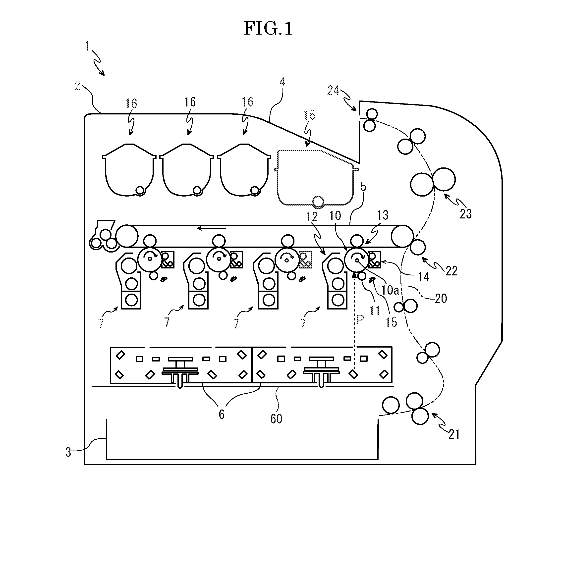
[0023]First, with reference to FIG. 1, the entire structure of a color printer 1 as an example of an electrographic image forming apparatus will be described. FIG. 1 is a schematic diagram schematically showing a color printer according to one embodiment of the present disclosure. In the following description, a left side in FIG. 1 shows a front side of the printer 1 and directions perpendicular to the forward and rearward directions seen from the front side show left and right directions.
[0024]The color printer 1 includes a box-like formed printer main body 2, a sheet feeding cassette 3 storing sheets (not shown) is provided in a lower part of the printer main body 2 and an ejected sheet tray 4 is formed on an upper end of the printer main body 2.
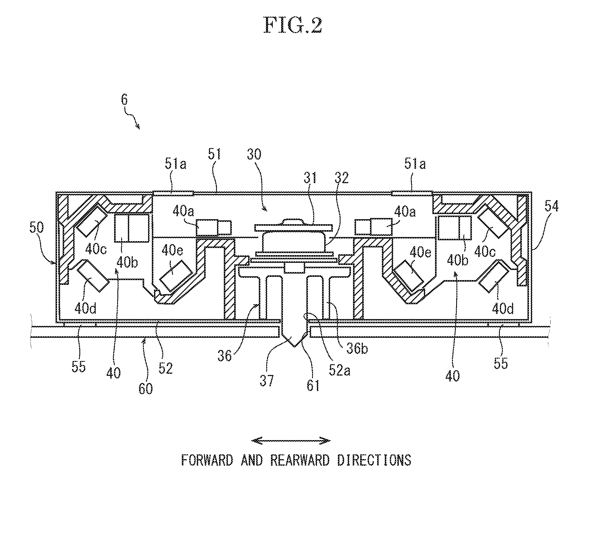
[0025]In an upper part of the printer main body 2, an intermediate transferring belt 5 is bridged between a plurality of rollers, and under the intermediate transferring belt 5, two scanning optical devices 6 each composing of a laser scan...
second embodiment
[0059]Next, a scanning optical device of a color printer as an image forming apparatus according to a second embodiment of the present invention will be described with reference to FIGS. 5 to 6. FIG. 5 is a perspective view showing a scanning optical device and a frame and FIG. 6 is a sectional side view of the scanning optical device.
[0060]Two scanning optical devices 100, as shown in FIG. 5 (only one is shown in FIG. 5), are mounted side by side in the forward and rearward directions to a frame 101 extending in the forward and rearward directions under the image forming parts 7 in the printer main body 2 (refer to FIG. 1).
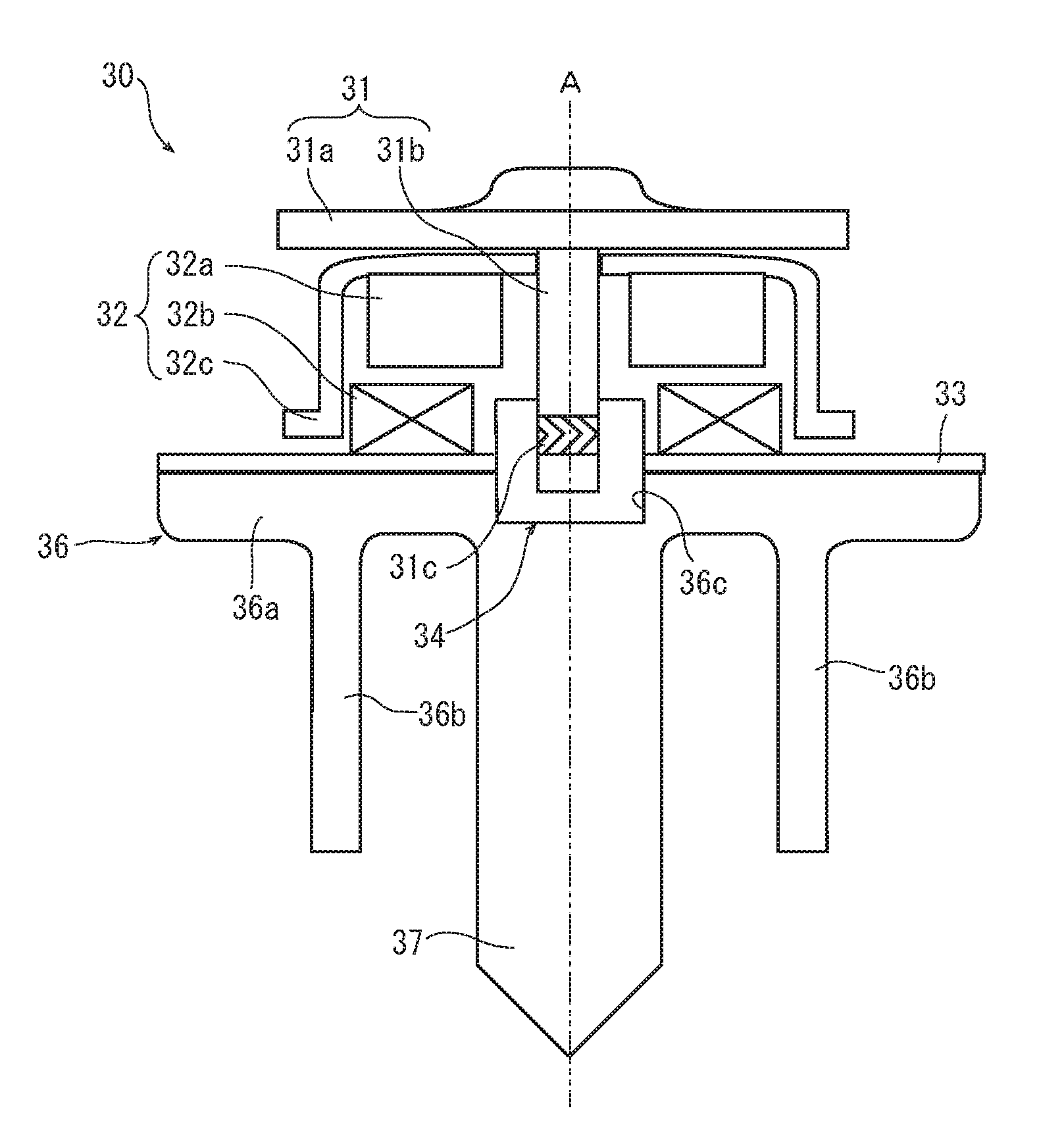
[0061]The scanning optical device 100, as shown in FIG. 6, has two light sources (not shown), a deflector 30, a heat sink 36, a pair of optical components groups 40, and an optical box 102 in which the light sources and the deflector 30, the heat sink 36, and the pair of optical components groups 40 are housed. The light sources, the heat sink 36, the deflector 3...
PUM
 Abstract
Description
Claims
Application Information


