Display arrangement and method for fabrication of a display arrangement

Active Publication Date: 2016-09-22
STMICROELECTRONICS INT NV
View PDF3 Cites 4 Cited by
  • Summary
  • Abstract
  • Description
  • Claims
  • Application Information

AI Technical Summary

Benefits of technology

[0043]The ferrite layer and the conductive shield advantageously realize a methodology to reduce electric and magnetic influences from the display to the antenna and vice versa.
[0044]In an embodiment, the conduc

Problems solved by technology

Normal operation of a display, such as a liquid crystal display, generates a large amount of noise in close proximity to the display due to the

Method used


Image

  • Display arrangement and method for fabrication of a display arrangement
  • Display arrangement and method for fabrication of a display arrangement
  • Display arrangement and method for fabrication of a display arrangement

Examples


Embodiment Construction

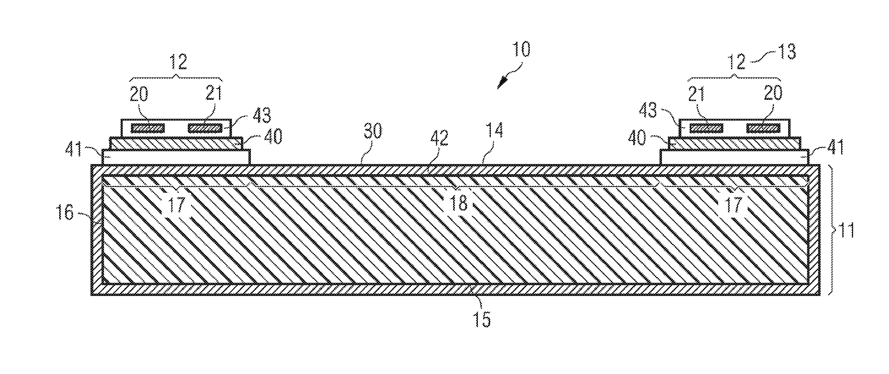
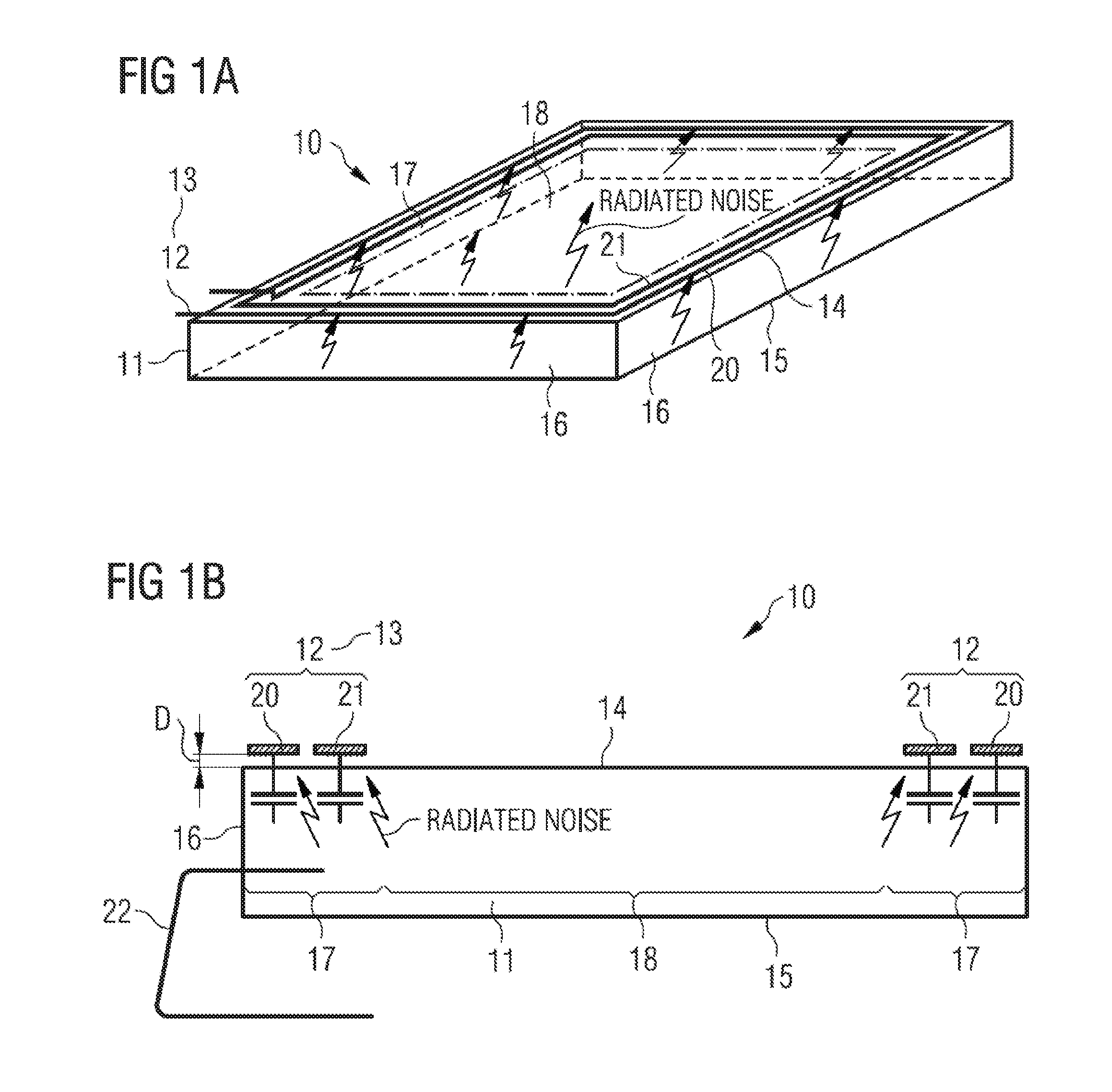
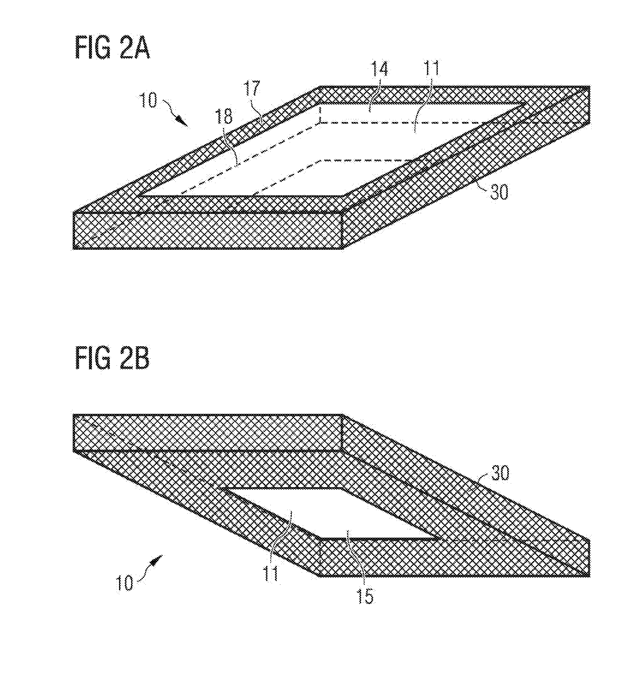
[0054]FIG. 1A shows an exemplary embodiment of a display arrangement 10 comprising a display 11 and a conducting line 12. The display 11 is realized as a housed display. The display 11 already comprises an enclosure, for example a plastic enclosure. The display 11 may be implemented as a liquid crystal display, abbreviated to LCD. The display 11 is unshielded.

[0055]The conducting line 12 forms an antenna 13. The conducting line 12 can also be called an antenna trace. The conducting line 12 realizes HF coil conductive traces. The antenna 13 is realized as HF antenna. The antenna 13 is implemented as a planar antenna. The conducting line 12 comprises at least one turn. In the example shown in FIG. 1A, the conducting line 12 performs two turns. The antenna 13 is realized as a coil-shaped antenna. The antenna 13 is used for RFID. The conducting line 12 and thus the antenna 13 are arranged on a first main surface 14 of the display 11. The unshielded LCD 11 has the HF antenna 13 on top of...


PUM


Abstract

A display arrangement comprises a display, a conductive shield arranged at the display, a ferrite layer and a conducting line of an antenna. The ferrite layer is arranged between the conducting line and the conductive shield.

Description

BACKGROUND OF THE INVENTION[0001]The present invention is related to a display arrangement and to a method for fabrication of a display arrangement.[0002]Normal operation of a display, such as a liquid crystal display, generates a large amount of noise in close proximity to the display due to the signals used during operation. The noise may have a disruptive impact on other systems, such as a radio frequency identification receiver system. In order to allow correct operation of the radio frequency identification system and, in particular, to guarantee a correct reception of data transmitted to a reader, the coupling effect between the liquid crystal display and an RF antenna has to be reduced.[0003]Document US 2009 / 0179806 A1 refers to the mounting of an antenna for electronic devices. A display casing comprises a non-conductive resin region having an antenna mounting space disposed therein and a display module accommodated in the display casing.[0004]Document US 2011 / 0156969 A1 des...

Claims


Application Information

Patent Timeline
IPC IPC(8): H01Q1/52H01Q7/06G06K7/10H01Q1/22
CPCH01Q1/526G06K7/10366H01Q7/06H01Q1/2216G02F1/13338G02F1/13394G02F1/1358G06F3/041G06F2203/04107G06K7/10297G02F1/13398
Inventor MANZI, GIULIANO
Owner STMICROELECTRONICS INT NV
Why Eureka
Try Eureka