
Scan driving circuit and LCD device

a driving circuit and driving circuit technology, applied in the field of display devices, can solve the problems of poor signal fluctuation of current scanning lines, affect the stability of the goa circuit, etc., and achieve the effects of improving work efficiency, enhancing stability of the goa, and affecting display quality

Active Publication Date: 2016-09-29
TCL CHINA STAR OPTOELECTRONICS TECH CO LTD
View PDF1 Cites 13 Cited by
  • Summary
  • Abstract
  • Description
  • Claims
  • Application Information

AI Technical Summary

Benefits of technology

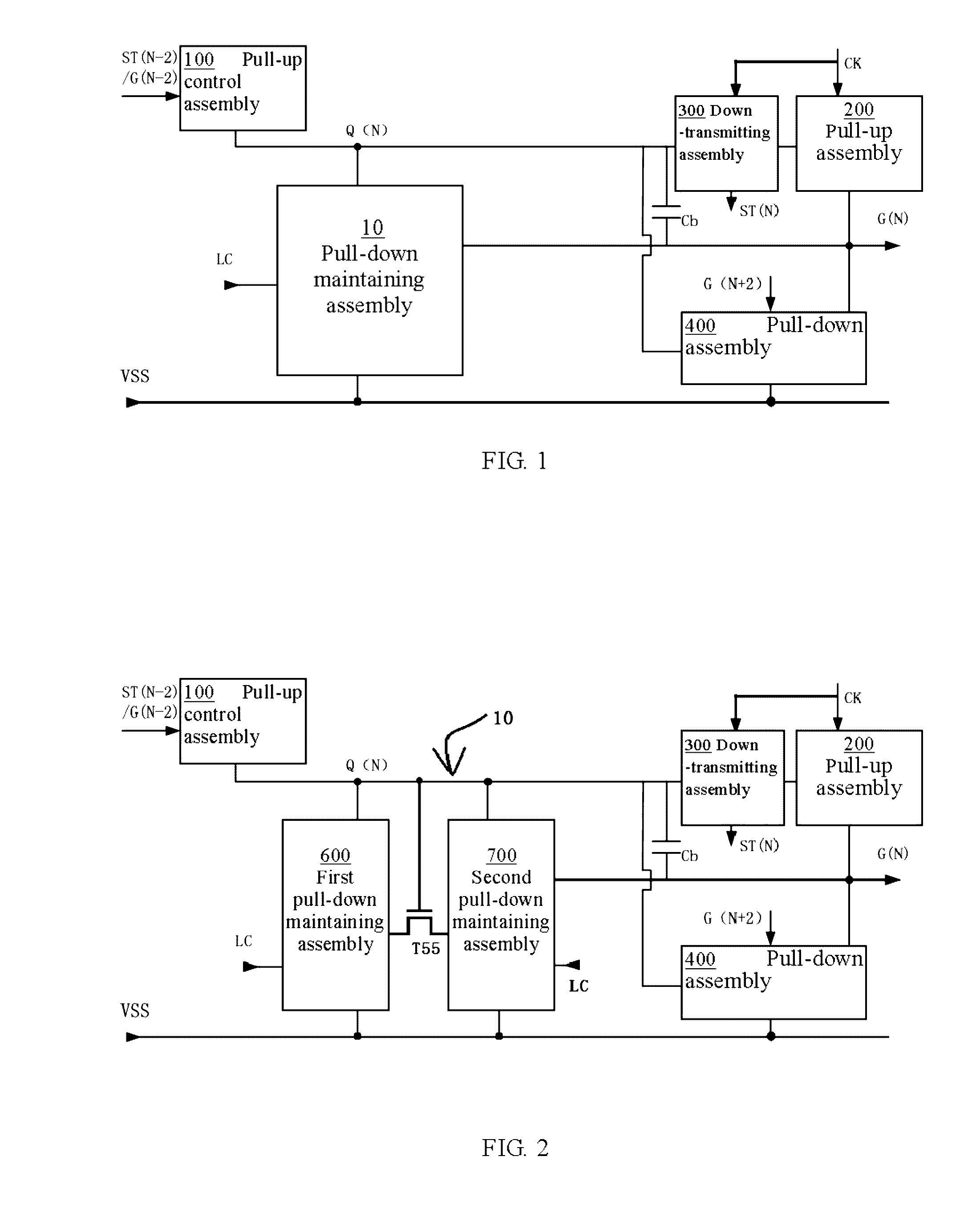
The present disclosure provides a scan driving circuit and a liquid crystal display (LCD) device that improve the stability of a gate driver on array (GOA) circuit. The technical effect of the patent is to provide a more stable and reliable circuit for driving the next scanning line, even if the current scanning line is not working properly. This is achieved by using a down-transmitting assembly that generates a down-transmitting signal that is independent for the circuit of the next GOA, ensuring steady working of the current scanning line and improving the stability of the GOA.

Problems solved by technology

Signal fluctuation of the current scanning line is not good for the current scanning line and start-up of the next-staged GOA circuit, and even affects stability of the GOA circuits.

Method used


Image

  • Scan driving circuit and LCD device
  • Scan driving circuit and LCD device
  • Scan driving circuit and LCD device

Examples


example 1

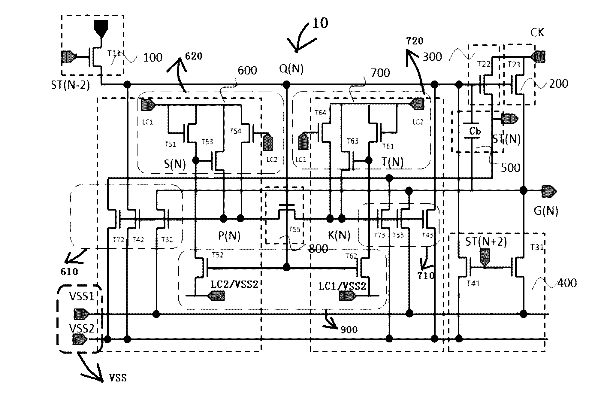
[0060]FIG. 2 is a schematic diagram of a first example of the present disclosure. In FIGS. 1-2, the pull-down maintaining assembly 10 comprises a first pull-down maintaining assembly 600 and a second pull-down maintaining assembly 700. Input ends of the first pull-down maintaining assembly 600 and the second pull-down maintaining assembly 700 are coupled to the output end Q(N) of the pull-up control assembly 100, the pull-down maintaining signal LC is sent to control ends of the first pull-down maintaining assembly 600 and the second pull-down maintaining assembly 700, and the reference low-level signal VSS is sent to output ends of the first pull-down maintaining assembly 600 and the second pull-down maintaining assembly 700.

[0061]The scan driving circuit further comprises a diverter switch T55 connected between the control ends of the first pull-down maintaining assembly 600 and the second pull-down maintaining assembly 700, and a control end of the diverter switch T55 is coupled ...

example 2

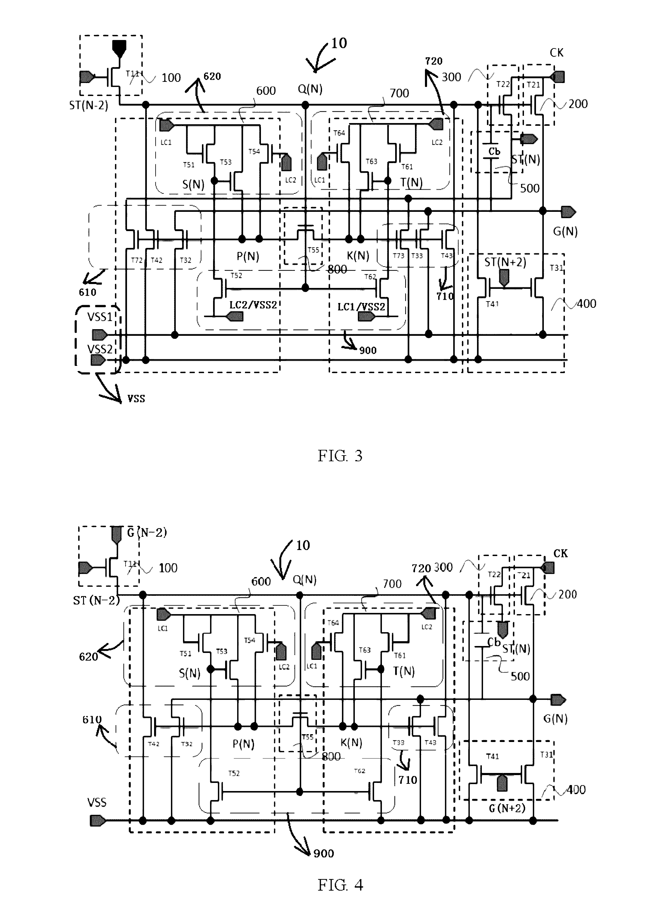
[0064]FIG. 3 is a schematic diagram of a second example of the present disclosure, and a detailed view of FIG. 1, the first pull-down maintaining assembly 600 comprises a first pull-down maintaining unit 610 and a first pull-down maintaining control unit 620 that drives the first pull-down maintaining unit 610. The first pull-down maintaining unit 610 comprises a first controllable switch T32 and a second controllable switch T42. The pull-down maintaining signal LC comprises a first pull-down maintaining signal LC1, and the first pull-down maintaining signal LC1 is sent to control ends of the first controllable switch T32 and the second controllable switch T42 via the first pull-down maintaining control unit 620. The reference low-level signal VSS is sent to the current scanning line G(N) via the first controllable switch T32, and is sent to the output end Q(N) of the pull-up control assembly 100 via the second controllable switch T42.

[0065]The down-transmitting assembly 300 compris...

example 3

[0084]FIG. 4 is a schematic diagram of a third example of the present disclosure, In FIG. 1 and FIG. 4, FIG. 4 is an detailed view of FIG. 1, the pull-down maintaining assembly 10 comprises the first pull-down maintaining assembly 600 comprising the first pull-down maintaining unit 610 and the first pull-down maintaining control unit 620, where the first pull-down maintaining control unit 620 drives the first pull-down maintaining unit 610. The first pull-down maintaining unit 610 comprises the first controllable switch T32 and the second controllable switch T42. The pull-down maintaining signal LC comprises the first pull-down maintaining signal LC1, and the first pull-down maintaining signal LC1 is sent to the control ends of the first controllable switch T32 and the second controllable switch T42 via the first pull-down maintaining control unit 620. The reference low-level signal VSS is sent to the current scanning line G(N) via the first controllable switch T32, and is sent to t...


PUM


Abstract

A scan driving circuit and a liquid crystal display device include a pull-up assembly, a pull-up control assembly that drives the pull-up assembly, a pull-down maintaining assembly, a reference low-level signal, and a down-transmitting assembly. A control end of the down-transmitting assembly is coupled to an output end of the pull-up control assembly and a control end of the pull-up assembly, and a current down-transmitting signal is output from an output end of the down-transmitting assembly.

Description

TECHNICAL FIELD[0001]The present disclosure relates to the field of display devices, and more particularly to a scan driving circuit and a liquid crystal display (LCD) device.BACKGROUND[0002]In typical gate driver on array (GOA) circuits, a next-staged GOA circuit is mostly driven by a current scanning line G(N) of a current GOA circuit, which affects the current scanning line G(N), and makes signals of the current scanning line fluctuate. Signal fluctuation of the current scanning line is not good for the current scanning line and start-up of the next-staged GOA circuit, and even affects stability of the GOA circuits.SUMMARY[0003]The aim of the present disclosure is to provide a scan driving circuit and a liquid crystal display (LCD) device capable of improving stability of a gate driver on array (GOA) circuit.[0004]The aim of the present disclosure is achieved by the following methods.[0005]A scan driving circuit includes a pull-up assembly, a pull-up control assembly that drives ...

Claims


Application Information

Patent Timeline
Patent Type & Authority Applications(United States)
IPC IPC(8): G09G3/36
CPCG09G3/3677G09G2310/08G09G2310/06G09G2300/0408G09G3/36
Inventor DAI, CHAO
Owner TCL CHINA STAR OPTOELECTRONICS TECH CO LTD
Learn More