Semiconductor module and semiconductor device
a semiconductor module and semiconductor technology, applied in the direction of semiconductor devices, semiconductor/solid-state device details, electrical apparatus, etc., can solve problems such as malfunctions in semiconductor modules, and achieve the effect of suppressing deterioration in the characteristics of semiconductor devices and preventing malfunctions
- Summary
- Abstract
- Description
- Claims
- Application Information
AI Technical Summary
Benefits of technology
Problems solved by technology
Method used
Image
Examples
first embodiment
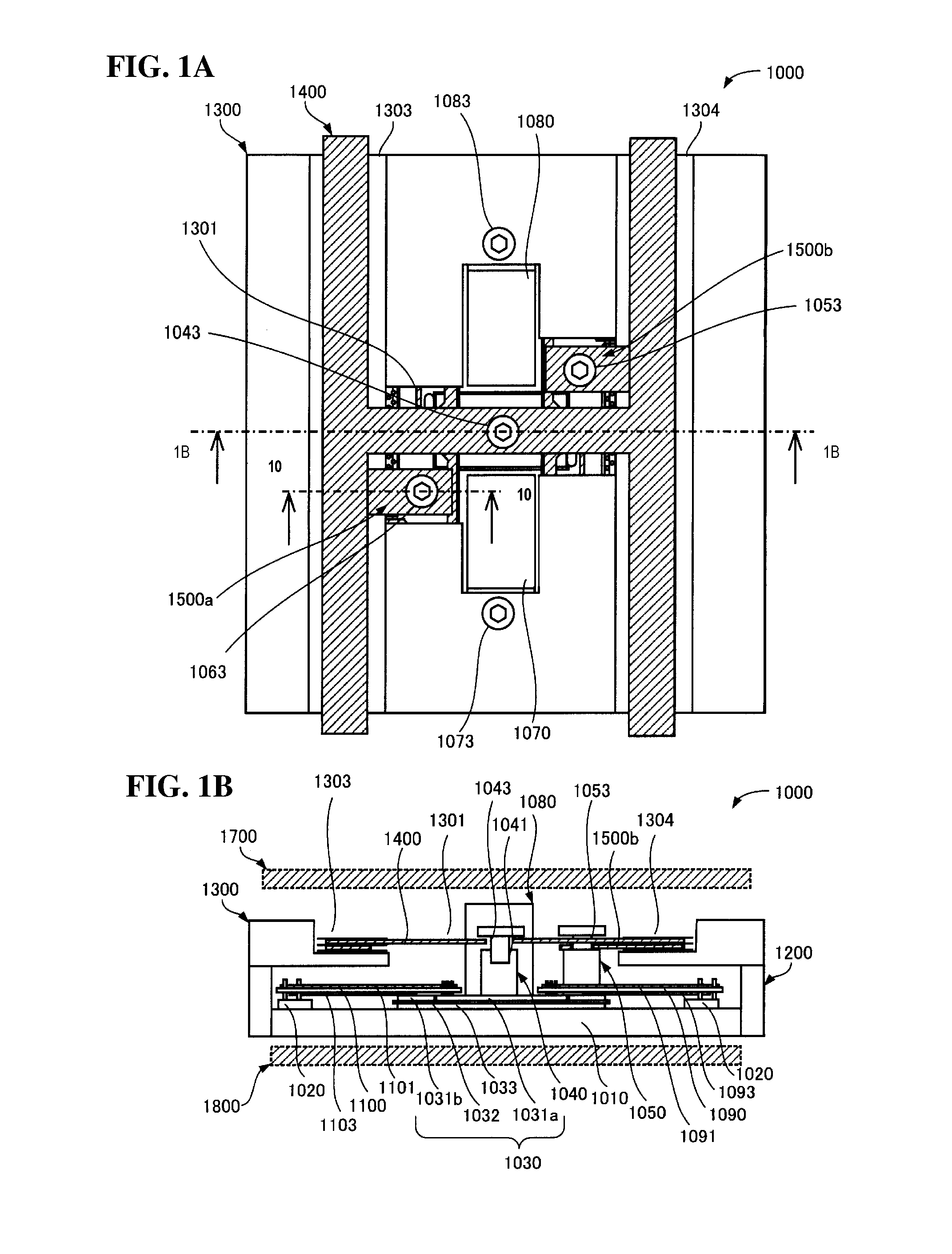
[0034]A description will be given, using FIGS. 1A to 10, of a semiconductor module of a first embodiment.
[0035]FIGS. 1A and 1B are diagrams showing the semiconductor module of the first embodiment.
[0036]FIG. 1A shows a plan view of the semiconductor module, and FIG. 1B shows a sectional view on the dashed dotted line X1-X1 of FIG. 1A.
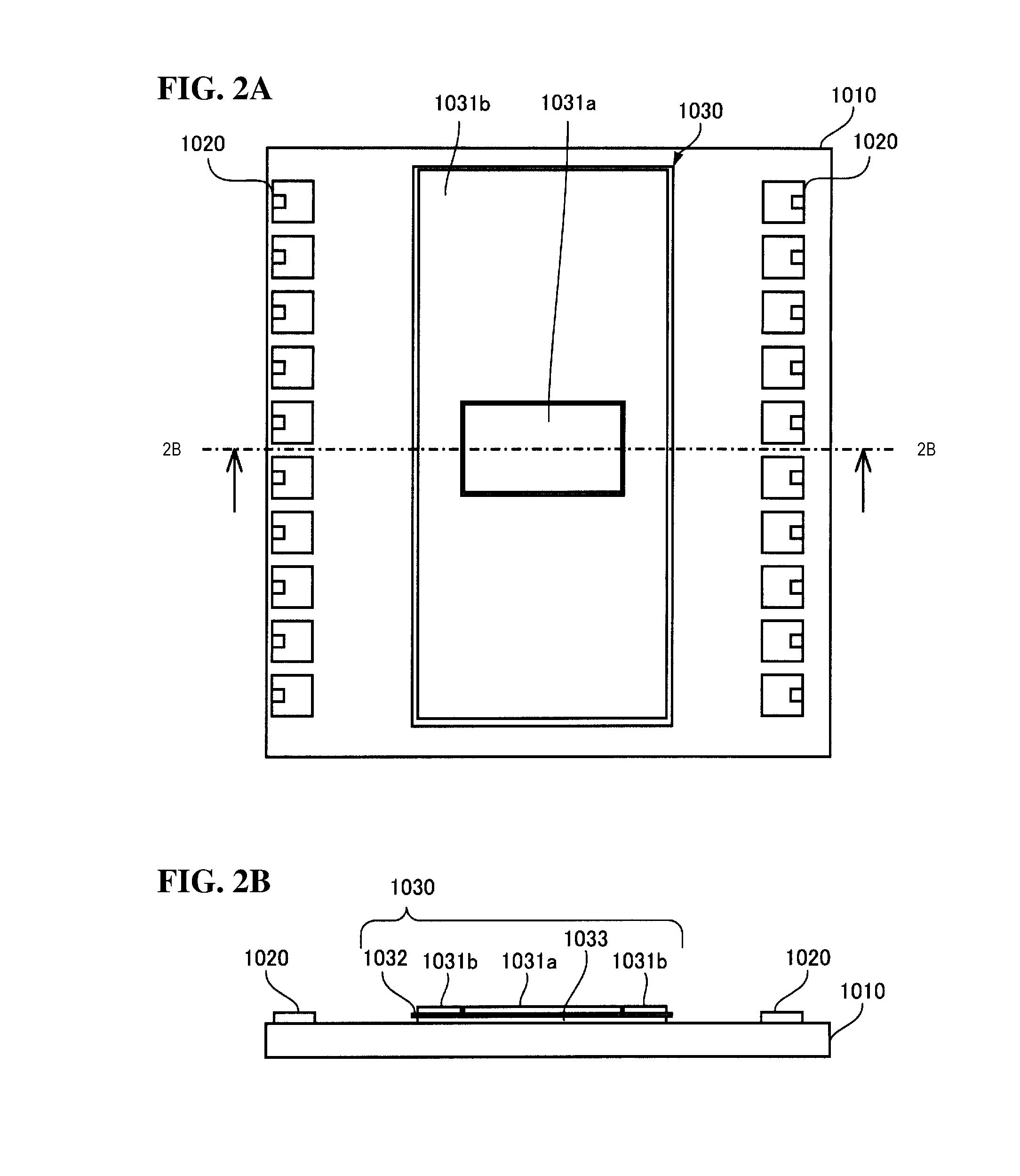
[0037]Also, FIGS. 2A to 10 are diagrams showing configurations of the semiconductor module of the first embodiment.
[0038]FIG. 2A shows a plan view of a drain plate 1010, and FIG. 2B shows a sectional view on the dashed dotted line X-X of FIG. 2A.
[0039]FIG. 3A shows a plan view of the drain plate 1010, FIG. 3B shows a side view in the direction of the arrow 3B of FIG. 3A, and FIG. 3C shows a side view in the direction of the arrow 3C of FIG. 3A.
[0040]FIG. 8A shows a plan view of a cover 1300, and FIG. 8B shows a perspective view of the semiconductor module (in which no gate plate 1400 or auxiliary source plates 1500a and 1500b are disposed).
[0041]FIG. 9A...
second embodiment
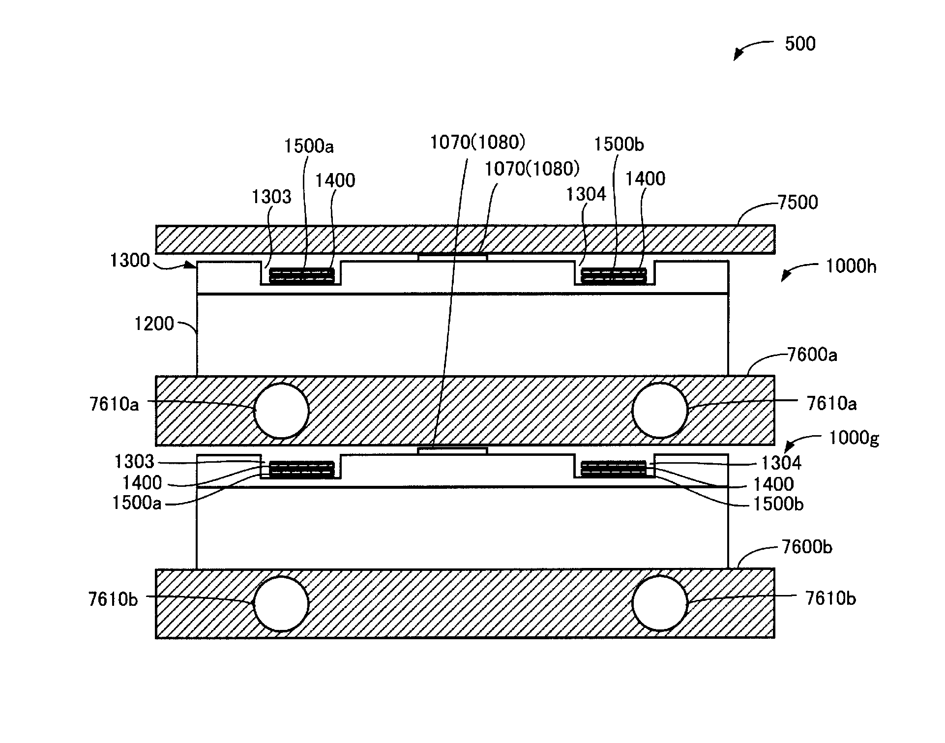
[0080]In a second embodiment, a description will be given, using FIGS. 11, 12A, and 12B, of a semiconductor device into which a plurality of the semiconductor modules shown in the first embodiment is combined.
[0081]FIG. 11 is a diagram showing a semiconductor device of the second embodiment.
[0082]Also, FIGS. 12A and 12B are diagrams showing wiring plates of the semiconductor device of the second embodiment.
[0083]FIG. 12A shows a plan view of a gate plate, and FIG. 12B shows a plan view of auxiliary source plates.
[0084]A plurality (in the second embodiment, three) of the semiconductor modules (FIG. 8B) is prepared, and is disposed so that the guide grooves 1303 are linked and the guide grooves 1304 are linked.
[0085]For the plurality of semiconductor modules with the guide grooves linked in this way, an integrated gate plate 2400 and integrated auxiliary source plates 2500a and 2500b as shown in FIGS. 12A and 12B are prepared.
[0086]The integrated auxiliary source plate 2500a is dispos...
third embodiment
[0092]In a third embodiment, a description will be given, using FIGS. 13A and 13B, of a semiconductor module wherein it is possible to obtain an auxiliary source current without providing any auxiliary source terminal.
[0093]FIGS. 13A and 13B are diagrams showing a semiconductor module of the third embodiment.
[0094]FIG. 13A shows a plan view of a cover 2300, and FIG. 13B shows a plan view of a semiconductor module 2000 of the third embodiment.
[0095]In the semiconductor module 2000, the auxiliary source terminals 1050 and 1060 shown in the semiconductor module 1000 of the first embodiment are not disposed. Also, as shown in FIG. 13A, an opening 2301 to expose the source terminals 1070 and 1080 and the gate terminal 1040 is formed in the cover 2300 of the semiconductor module 2000. Furthermore, the cover 2300 includes depressed portions 2302 and 2303, which are positioned at the same depth (height) as the guide grooves 1303 and 1304, and bolt holes 2306 and 2307 provided in the depress...
PUM
 Abstract
Description
Claims
Application Information
 - R&D
- Intellectual Property
- Life Sciences
- Materials
- Tech Scout
- Unparalleled Data Quality
- Higher Quality Content
- 60% Fewer Hallucinations
Browse by: Latest US Patents, China's latest patents, Technical Efficacy Thesaurus, Application Domain, Technology Topic, Popular Technical Reports.
© 2025 PatSnap. All rights reserved.Legal|Privacy policy|Modern Slavery Act Transparency Statement|Sitemap|About US| Contact US: help@patsnap.com


