Identification circuit and IC chip comprising the same

a technology of identification circuit and ic chip, which is applied in the field of integrated circuit (ic) chips, can solve the problems of inability to duplicate, increase cost and time expense, and not be good for key generation or similar security applications, so as to avoid unnecessarily

Inactive Publication Date: 2016-10-13
CASINDA INC
View PDF10 Cites 3 Cited by
  • Summary
  • Abstract
  • Description
  • Claims
  • Application Information

AI Technical Summary

Benefits of technology

[0017]The above features and advantages and other features and advantages of the present invention are readily apparent from the following detailed description of the best modes for carrying out the invention when taken in connection with the accompanying drawings.
[0018]The present invention is illustrated by way of example, and not by way of limitation, in the figures of the accompanying drawings and in which like reference numerals refer to similar elements. All the figures are schematic and generally only show parts which are necessary in order to elucidate the invention. For simplicity and clarity of illustration, elements shown in the figures and discussed below have not necessarily been drawn to scale. Well-known structures and devices are shown in simplified form such as block diagrams in order to avoid unnecessarily obscuring the present invention. Other parts may be omitted or merely suggested.

Problems solved by technology

While such a method can provide each chip with a customized ID number to uniquely identify the chip and provide further information about the chip, they require special processing steps when manufacturing the chip and thus incur additional cost and time expense.
In addition, the ID number may be easily altered or cloned, so it is not good for key generation or similar security applications.
PUFs are especially suitable for security applications, because they are easy to generate but practically, they are impossible to duplicate, even using the exact manufacturing process to produce them.
A disadvantage of SRAM PUF is its insufficient stability.
As a result, the process variations may be very small.
On the other hand, noise from adjacent circuits or from external environment may have an impact on the output of the SRAM cells.
Therefore, some of the SRAM cells may have random output, causing the generated ID number inconstant.
This has become a serious obstacle that hinders SRAM PUF from being used in on-chip ID circuits.
Therefore, the SRAM PUF results in a significant decrease in layout flexibility and an increase in cost.

Method used


Image

  • Identification circuit and IC chip comprising the same
  • Identification circuit and IC chip comprising the same
  • Identification circuit and IC chip comprising the same

Examples


Embodiment Construction

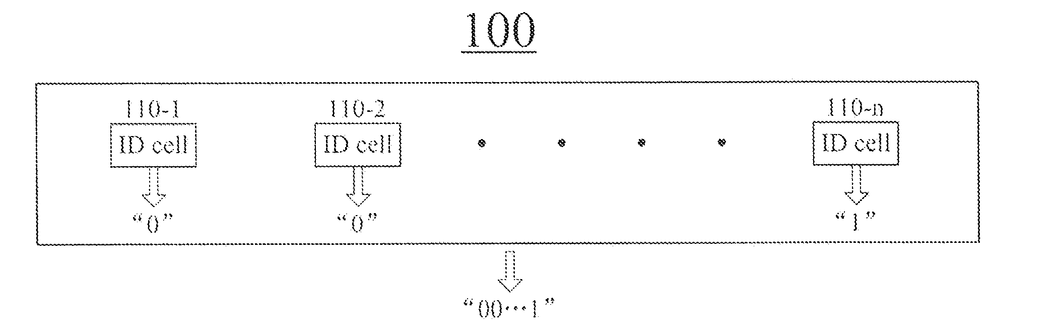
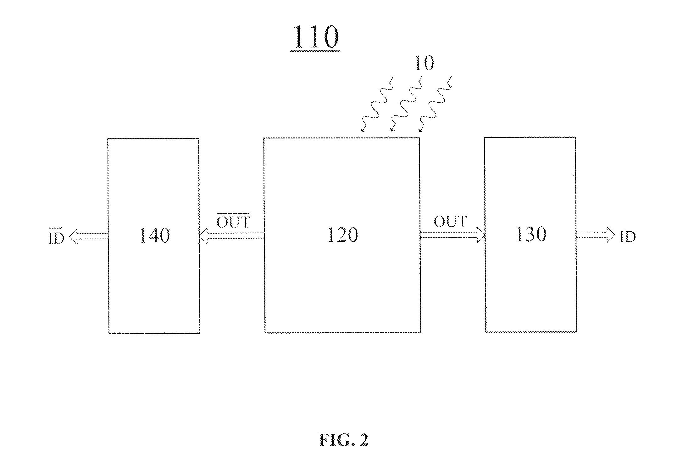
[0028]In the following description, for the purposes of explanation, numerous specific details are set forth in order to provide a thorough understanding of the present invention. It is apparent, however, to one skilled in the art that the present invention may be practiced without these specific details or with an equivalent arrangement.

[0029]It is also to be understood that the terminology used herein is for the purpose of describing particular embodiments only, and is not intended to limit the scope of the invention. For example, when an element is referred to as being “on”, “connected to”, or “coupled to” another element, it can be directly on, connected or coupled to the other element or intervening elements may be present. In contrast, when an element is referred to as being “directly on”, “directly connected to”, or “directly coupled to” another element, there are no intervening elements present.

[0030]Unless otherwise defined, all terms (including technical and scientific ter...


PUM


Abstract

An embodiment of the present invention is an identification circuit for generating an identification number (ID). The identification circuit includes a plurality of identification cells each comprising a latch having a first output and a second output that are opposite to each other. The first output and the second output are a function of process variations of the identification circuit. A first buffer and a second buffer are provided on both sides of the latch and connected to the first output and the second output of the latch, respectively.

Description

CROSS-REFERENCE TO RELATED U.S. APPLICATIONS[0001]Not applicable.STATEMENT REGARDING FEDERALLY SPONSORED RESEARCH OR DEVELOPMENT[0002]Not applicable.NAMES OF PARTIES TO A JOINT RESEARCH AGREEMENT[0003]Not applicable.REFERENCE TO AN APPENDIX SUBMITTED ON COMPACT DISC[0004]Not applicable.FIELD OF THE INVENTION[0005]The present invention generally relates to an integrated circuit (IC) chip, and more particularly, to an IC chip in which an identification circuit is inserted for generating a unique and non-alterable identification number (ID) identifying the IC chip.BACKGROUND OF THE INVENTION[0006]An identification number (ID) is often desirable for many IC chips or electronic devices. Just like DNA, the ID number can uniquely identify an IC chip or an electronic device containing the IC chip and distinguish it from others, thereby improving recognizability and traceability of products. Moreover, the ID number may be used, for example, to label RFID tags, to generate public or private k...

Claims


Application Information

Patent Timeline
Patent Type & Authority Applications(United States)
IPC IPC(8): H03K19/094G01R31/3177
CPCG01R31/3177H03K19/094H01L23/544H01L2223/54433H01L2224/49113H01L2924/00H01L2924/00014H01L2924/13091
Inventor XIAO, JIMMY YONGRATHAUR, SURENDRA KUMARYEGNASHANKARAN, VISVAMOHAN
Owner CASINDA INC
Why Eureka
Try Eureka