Pixel circuit of organic light emitting diode display device for compensating for a characteristic deviation of a driving thin film transistor

a technology of organic light-emitting diodes and display devices, which is applied in the direction of static indicating devices, instruments, etc., can solve the problems of uneven luminance, reduced luminance, and reduced lifespan, and achieve the effect of minimizing the influence of previous frames

Active Publication Date: 2015-03-17
LG DISPLAY CO LTD
View PDF8 Cites 26 Cited by
  • Summary
  • Abstract
  • Description
  • Claims
  • Application Information

AI Technical Summary

Benefits of technology

[0013]An object of the present invention is to provide a pixel circuit of an organic light emitting diode display device which is capable of preventing an organic light emitting diode from unnecessarily emitting light even under the condition of removing a light-emission switching thin film transistor, and minimizing the influence of a previous frame.

Problems solved by technology

However, a conventional pixel circuit has a disadvantage in that the threshold voltage Vth of a driving TFT is non-uniform by positions by reason of a process deviation, etc., resulting in unevenness in luminance, or the threshold voltage varies with time by the same reason, resulting in a reduction in luminance, thereby reducing lifespan.
However, in the conventional pixel circuit, the threshold voltage of the driving TFT can be compensated, but the threshold voltage of the light-emission switching TFT connected in series between the driving TFT and the OLED cannot be compensated, resulting in unevenness in luminance due to a difference in the threshold voltage of the light-emission switching TFT.
Also, in the conventional pixel circuit, the gate and source of the driving TFT may be influenced by data of a previous frame, thereby making accurate data input impossible.

Method used


Image

  • Pixel circuit of organic light emitting diode display device for compensating for a characteristic deviation of a driving thin film transistor
  • Pixel circuit of organic light emitting diode display device for compensating for a characteristic deviation of a driving thin film transistor
  • Pixel circuit of organic light emitting diode display device for compensating for a characteristic deviation of a driving thin film transistor

Examples


Embodiment Construction

[0032]Reference will now be made in detail to the preferred embodiments of the present invention, examples of which are illustrated in the accompanying drawings. Wherever possible, the same reference numbers will be used throughout the drawings to refer to the same or like parts.

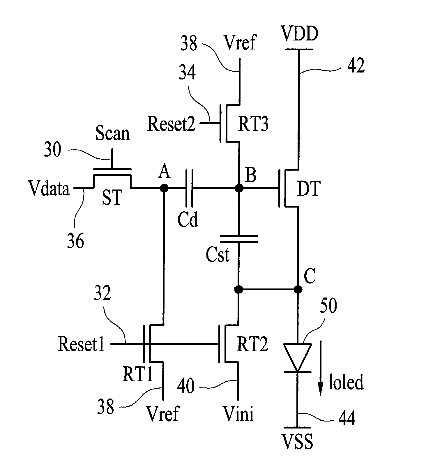
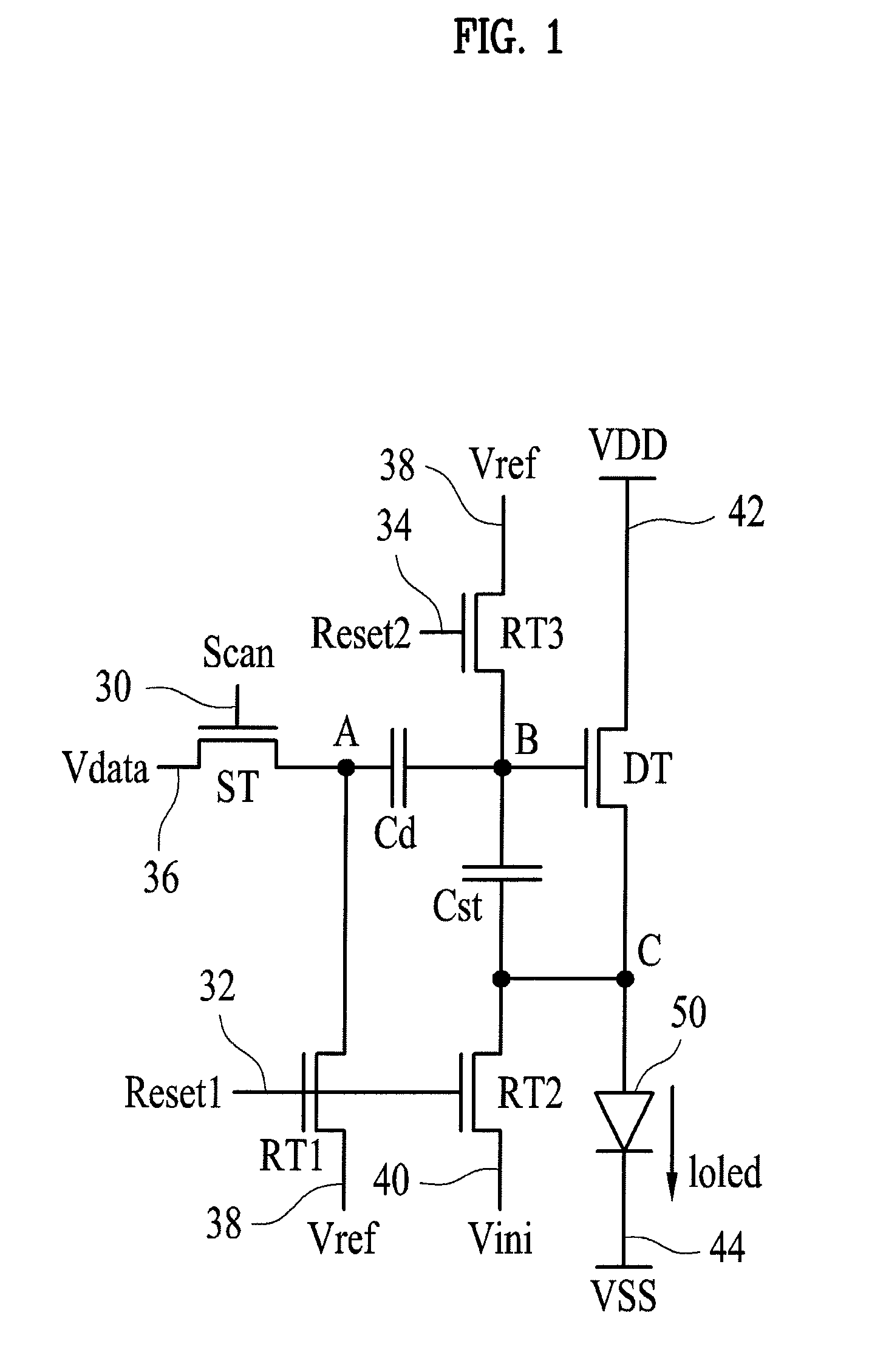
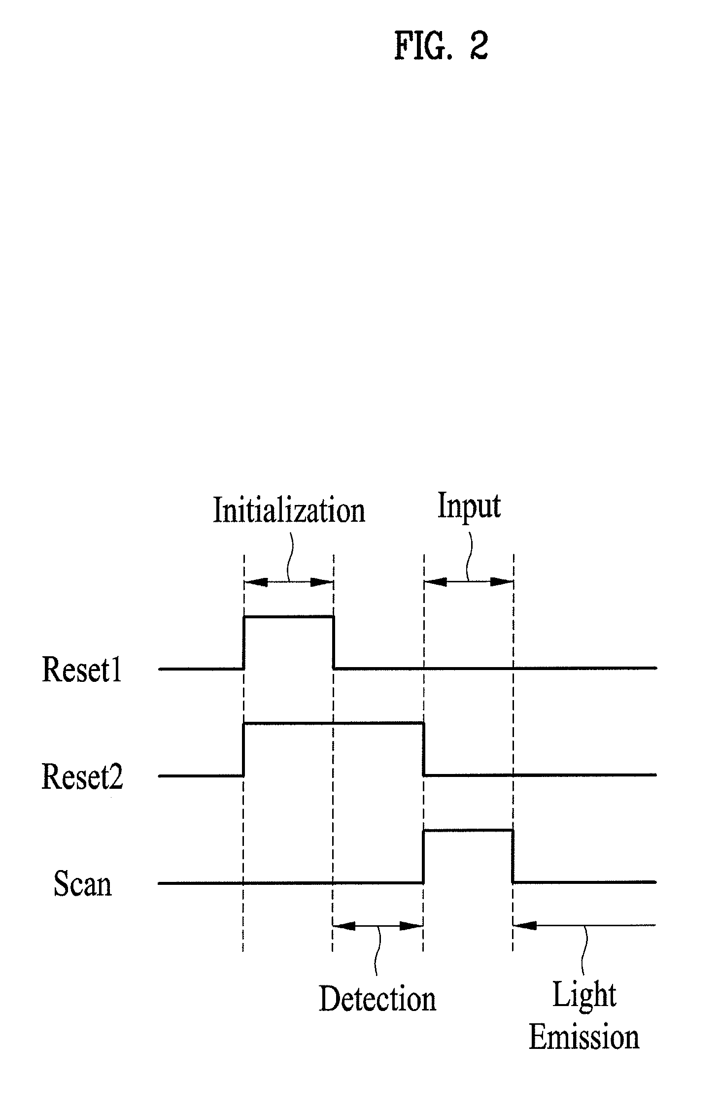
[0033]FIG. 1 is an equivalent circuit diagram of a pixel circuit of an OLED display device according to an embodiment of the present invention, and FIG. 2 is a driving waveform diagram of the pixel circuit of FIG. 1.

[0034]Referring to FIG. 1, in order to independently drive an OLED 50, the pixel circuit according to the present embodiment has a 5T2C structure consisting of five TFTs including a driving TFT DT, a switching TFT ST and first to third reset TFTs RT1, RT2 and RT3, and two capacitors including a storage capacitor Cst and a delivery capacitor Cd. Although all of the five TFTs DT, ST, RT1, RT2 and RT3 are illustrated in FIG. 1 as being of n type, they may be of p type.

[0035]Also, the pixel circuit s...


PUM


Abstract

A pixel circuit of an OLED display device is disclosed. The pixel circuit includes a light emitting element, a driving TFT for driving the light emitting element, a delivery capacitor connected between a first node and a second node, a storage capacitor connected between the second node and a third node, a first reset TFT for initializing the first node to a reference voltage in response to a first reset signal from a first reset line, a second reset TFT for initializing the third node to an initialization voltage in response to the first reset signal from the first reset line, a third reset TFT for initializing the second node to the reference voltage in response to a second reset signal from a second reset line, and a switching TFT for supplying a data voltage to the first node in response to a scan signal from a scan line.

Description

[0001]This application claims the benefit of Korean Patent Application No. 10-2011-0089883, filed on Sep. 5, 2011, which is hereby incorporated by reference as if fully set forth herein.BACKGROUND OF THE INVENTION[0002]1. Field of the Invention[0003]The present invention relates to an organic light emitting diode (referred to hereinafter as an OLED) display device, and more particularly, to a pixel circuit of an OLED display device which is capable of compensating for a characteristic deviation of a driving thin film transistor and reducing the influence of a previous frame.[0004]2. Discussion of the Related Art[0005]An OLED display device is a self-emissive device in which an organic light emitting layer emits light by recombination of electrons and holes, and is expected to be a next-generation display device in that it is high in luminance, low in driving voltage and ultra-thin in thickness.[0006]Such an OLED display device includes a plurality of pixels, each of which includes a...

Claims


Application Information

Patent Timeline
Patent Type & Authority Patents(United States)
IPC IPC(8): G09G3/30G09G3/10G09G3/32
CPCG09G3/3225G09G3/3291G09G2320/045G09G2300/0861G09G2300/0852G09G3/325H10K59/121H10K59/1213
Inventor LEE, YOUNG-HAKKIM, GEUN-YOUNG
Owner LG DISPLAY CO LTD
Why Eureka
Try Eureka