Self-Capacitance Touch Liquid Crystal Grating, Manufacturing Method Thereof, Driving Method Thereof, Display Panel and Display Device

a technology of liquid crystal grating and self-capacitance, which is applied in the field of touch technology, can solve the problems that the technique of in-cell touch implementation in a state of 3d display is rarely known by people, and achieve the effect of avoiding interference between the sensing electrode and the grating and reducing the loading of the sensing electrod

Active Publication Date: 2016-10-27
BOE TECH GRP CO LTD +1
View PDF2 Cites 2 Cited by
  • Summary
  • Abstract
  • Description
  • Claims
  • Application Information

AI Technical Summary

Benefits of technology

[0030]In the self-capacitance touch liquid crystal grating provided by the present invention, as the orthographic projections of the plurality of strip-shaped electrodes on the sensing electrode layer are respectively located in the plurality of row spacing areas or the plurality of column spacing areas formed through the plurality of sensing electrodes arranged in the matrix form, the sensing electrode-to-earth capacitance is located between the surface-shaped electrode and the sensing electrodes, and the strip-shaped electrode will not cause the sensing electrode-to-earth capacitance to be increased. Therefore, the RC loading of the sensing electrodes can be largely reduced, and also the interference between the sensing electrodes and the grating can be avoided, so that touch operations will not interfere with operations of the grating.

Problems solved by technology

However, a technique in which an in-cell touch is implemented in a state of 3D display is rarely known by people.
In the prior art, a bottleneck of implementing the in-cell touch in the state of 3D display is that a resistance-capacitance loading (RC loading) of a sensing electrode is increased by a surface-shaped electrode and a strip-shaped electrode of a 3D grating.
Meanwhile, a voltage signal on the sensing electrode interferes with deflection of liquid crystal in the 3D grating.
Hence, how to prevent the 3D grating and the sensing electrode from interfering with each other becomes a technical problem in the art, which needs to be solved urgently.

Method used


Image

  • Self-Capacitance Touch Liquid Crystal Grating, Manufacturing Method Thereof, Driving Method Thereof, Display Panel and Display Device
  • Self-Capacitance Touch Liquid Crystal Grating, Manufacturing Method Thereof, Driving Method Thereof, Display Panel and Display Device
  • Self-Capacitance Touch Liquid Crystal Grating, Manufacturing Method Thereof, Driving Method Thereof, Display Panel and Display Device

Examples


embodiment 1

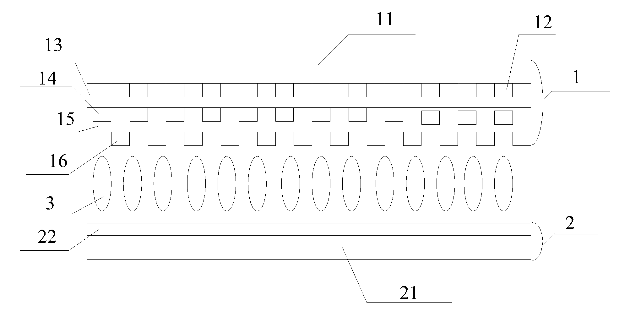
[0041]The present embodiment provides a self-capacitance touch liquid crystal grating, as shown in FIG. 1, it includes a first base substrate 1, a second base substrate 2 and a liquid crystal layer 3 that is filled between the first base substrate 1 and the second base substrate 2. The first base substrate 1 includes a first substrate 11, and a sensing electrode layer and a plurality of strip-shaped electrodes 16 arranged on a side of the first substrate 11 facing the liquid crystal layer 3, the sensing electrode layer being arranged to be insulated from the plurality of strip-shaped electrodes 16. The sensing electrode layer includes a plurality of sensing electrodes 12 arranged in a matrix form. The plurality of strip-shaped electrodes 16 are arranged in parallel and spaced. Orthographic projections of the plurality of strip-shaped electrodes 16 on the sensing electrode layer are respectively located in a plurality of row spacing areas or a plurality of column spacing areas formed...

embodiment 2

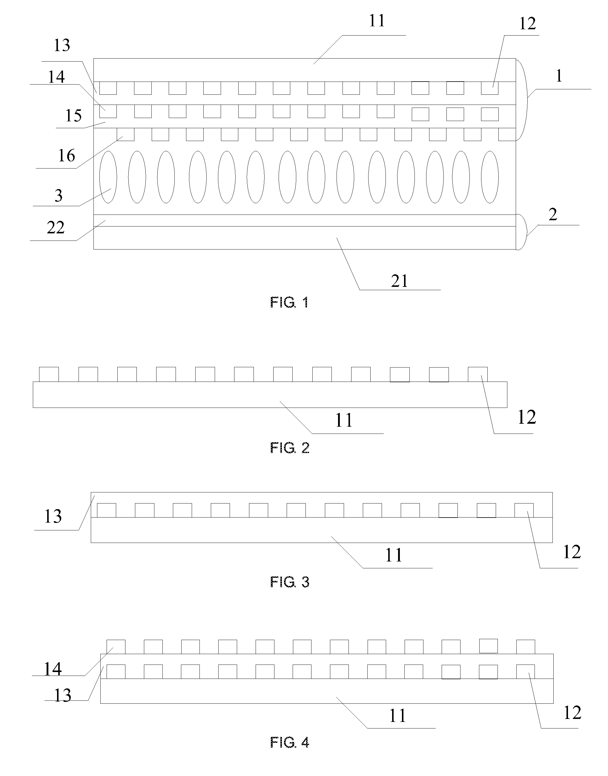
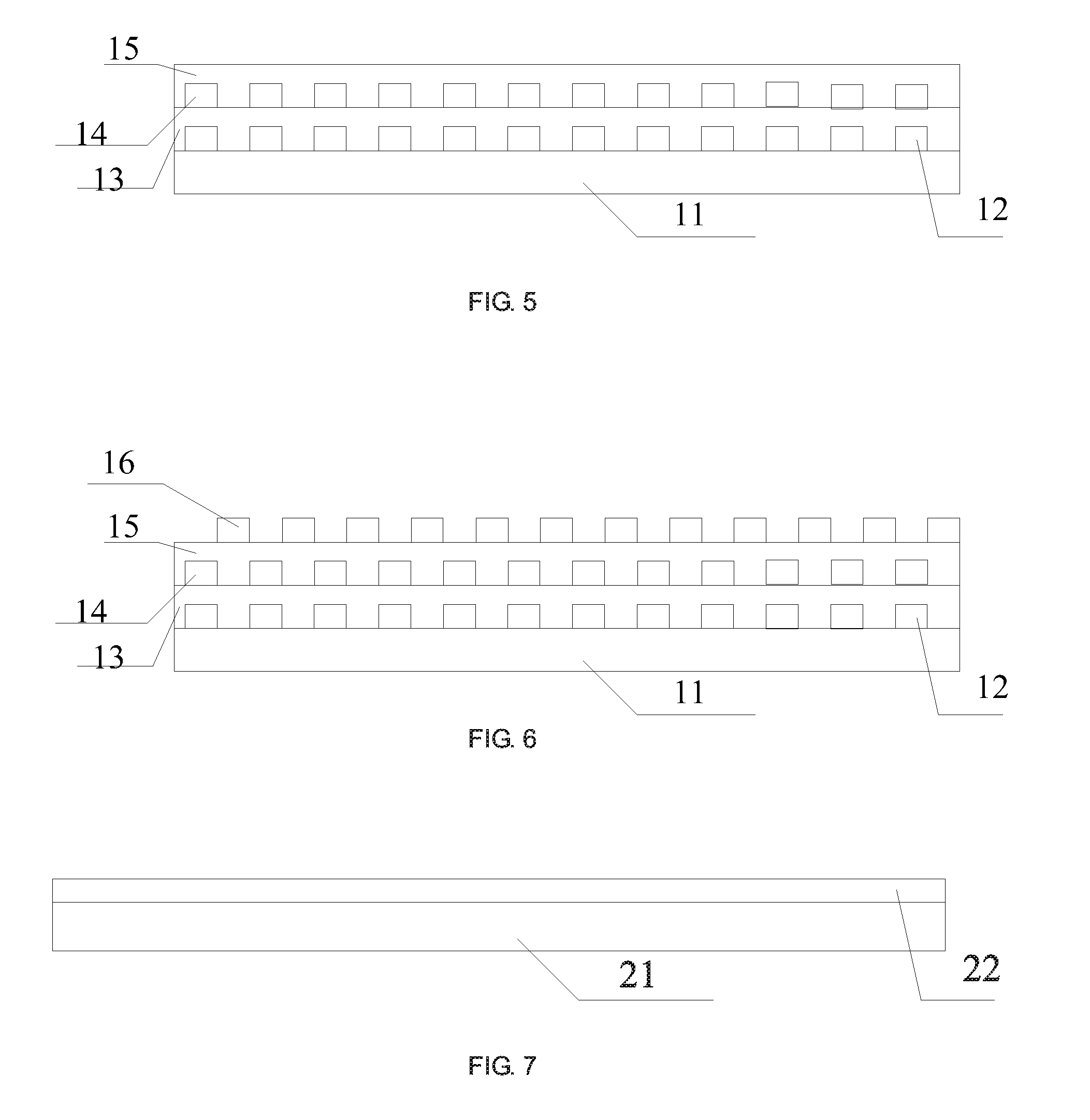
[0048]As shown in FIGS. 1-7, the present embodiment provides a manufacturing method of the self-capacitance touch liquid crystal grating of Embodiment 1, which includes the following steps S1 to S3.

[0049]At step S1, the first base substrate 1 is manufactured.

[0050]The step S1 specifically includes the following steps S11 to S15.

[0051]At step S11, as shown in FIG. 2, the sensing electrode layer is formed on the first substrate 11 by a patterning process, and the sensing electrode layer includes a plurality of sensing electrodes 12 arranged in a matrix form. In this embodiment, the sensing electrode 12 is a self-capacitance type sensing electrode, so that it will be sufficient if the plurality of sensing electrodes 12 are formed in the matrix form.

[0052]At step S12, as shown in FIG. 3, by a patterning process, the first insulation layer 13 is formed on the first substrate 11 formed with the plurality of sensing electrodes 12, and a plurality of via holes (not shown in the Figure) are ...

embodiment 3

[0059]As shown in FIG. 8, the present embodiment provides a driving method for the self-capacitance touch liquid crystal grating of Embodiment 1, including a step of alternately driving the sensing electrodes 12, the surface-shaped electrode 22 and the strip-shaped electrodes 16 during a display phase and a touch phase.

[0060]In the display phase: a first surface-shaped electrode driving voltage signal is input to the sensing electrodes 12 and the surface-shaped electrode 22, and a first grating driving voltage signal is input to the strip-shaped electrodes 16, such that an electric field capable of controlling the liquid crystal grating is generated between the surface-shaped electrode 22 and the strip-shaped electrodes 16, whereas there is no electric field between the sensing electrodes 12 and the surface-shaped electrode 22. Therefore, the control on the deflections of the liquid crystals by the electric field generated between the strip-shaped electrodes 16 and the surface-shape...


PUM

PropertyMeasurementUnit
electric fieldaaaaaaaaaa
self-capacitanceaaaaaaaaaa
driving voltageaaaaaaaaaa

Abstract

Embodiments of the invention provide a self-capacitance touch liquid crystal grating, a manufacturing method thereof, a driving method thereof, a self-capacitance touch liquid crystal 3D display panel, and a self-capacitance touch liquid crystal 3D display device. In the grating provided by embodiments of the present invention, as orthographic projections of strip-shaped electrodes on a sensing electrode layer are respectively located in row spacing areas or column spacing areas formed through sensing electrodes arranged in a matrix form, the sensing electrode-to-earth capacitance is located between a surface-shaped electrode and the sensing electrodes, and the strip-shaped electrode will not cause the sensing electrode-to-earth capacitance to be increased. Therefore, RC loading of the sensing electrodes can be largely reduced, and also the interference between the sensing electrodes and the grating can be avoided, so that touch operations will not interfere with operations of the grating.

Description

FIELD OF THE INVENTION[0001]The present invention relates to the field of touch technology, and particularly relates to a self-capacitance touch liquid crystal grating, a manufacturing method thereof, a driving method thereof, a display panel, and a display device.BACKGROUND OF THE INVENTION[0002]21st century is an era of information revolution, and the development of communication technology leads this information revolution. The pursuit of mobile communication products by people is changed from black-and-white displayed mobile communication product in the early days to color displayed mobile communication product, and at present, to touch mobile communication product. As the big data time is coming, 3D mobile communication product attracts people's attentions, and becomes future trend of development in the field of communication. However, a technique in which an in-cell touch is implemented in a state of 3D display is rarely known by people.[0003]In the prior art, a bottleneck of ...

Claims


Application Information

Patent Timeline
Patent Type & Authority Applications(United States)
IPC IPC(8): G02F1/1343G06F3/044G02F1/1333
CPCG02F1/134336G02F1/13338G06F2203/04103G06F3/044G02F1/13439G02B30/27G02F1/134309G06F3/04184G06F3/0445
Inventor DING, XIAOLIANGDONG, XUEWANG, HAISHENGLIU, YINGMINGLI, CHANGFENGREN, TAO
Owner BOE TECH GRP CO LTD
Why Eureka
Try Eureka