Thin film transistor substrate and display panel having the same

Active Publication Date: 2016-11-03
SAMSUNG DISPLAY CO LTD
View PDF0 Cites 11 Cited by
  • Summary
  • Abstract
  • Description
  • Claims
  • Application Information

AI Technical Summary

Benefits of technology

[0040]The display panel may include a barrier layer disposed on a base substrate, thereby preventing moisture from penetrating into a display device.
[0041]Since the difference between the refractive index of the barrier layer and the refractive index of the base substrate is small, the light may be prevented from being reflected at an interface between the barrier layer and the base substrate. Accordingly, the light transmittanc

Problems solved by technology

Further, some display devices

Method used


Image

  • Thin film transistor substrate and display panel having the same
  • Thin film transistor substrate and display panel having the same
  • Thin film transistor substrate and display panel having the same

Examples


Embodiment Construction

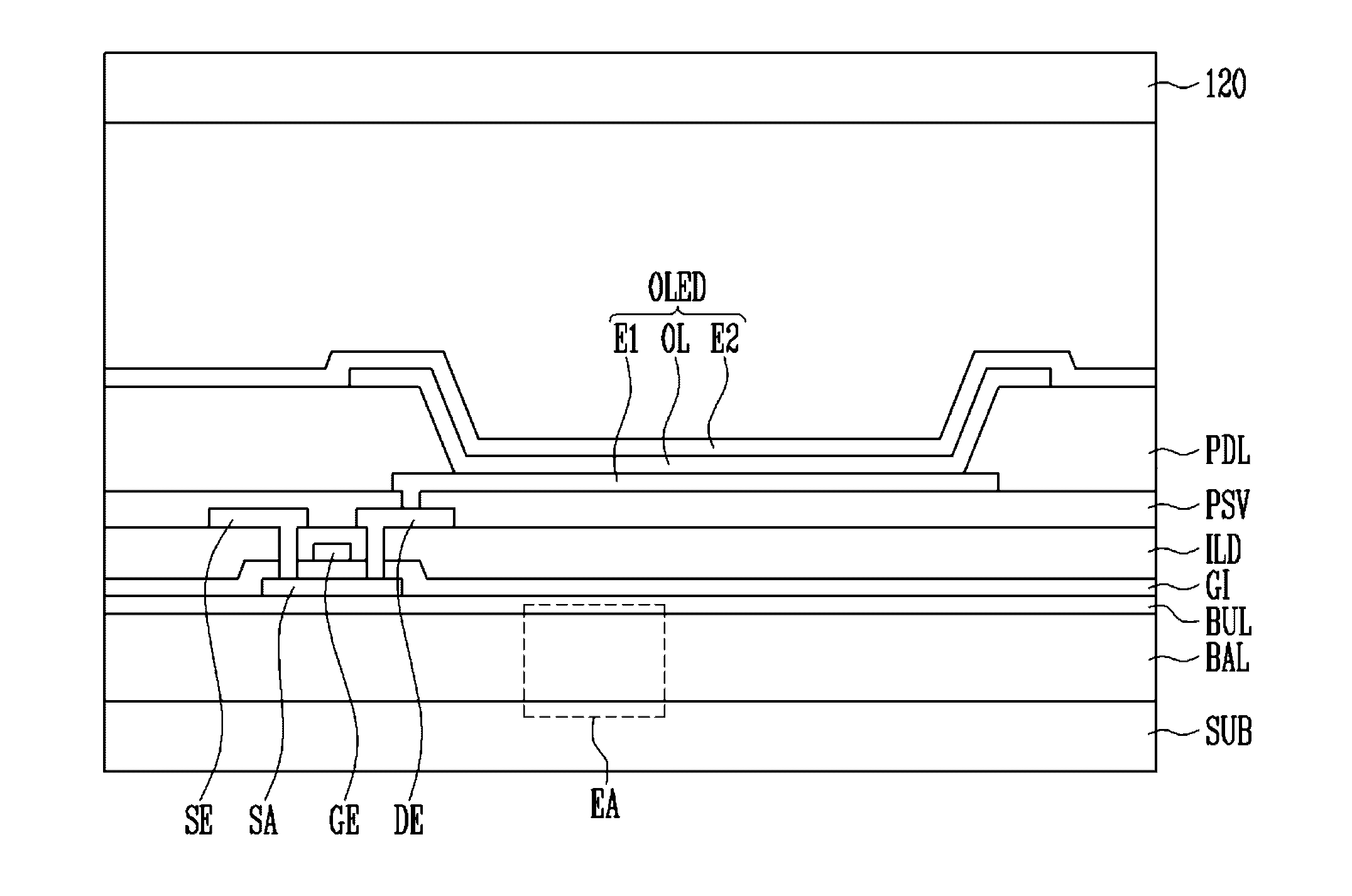
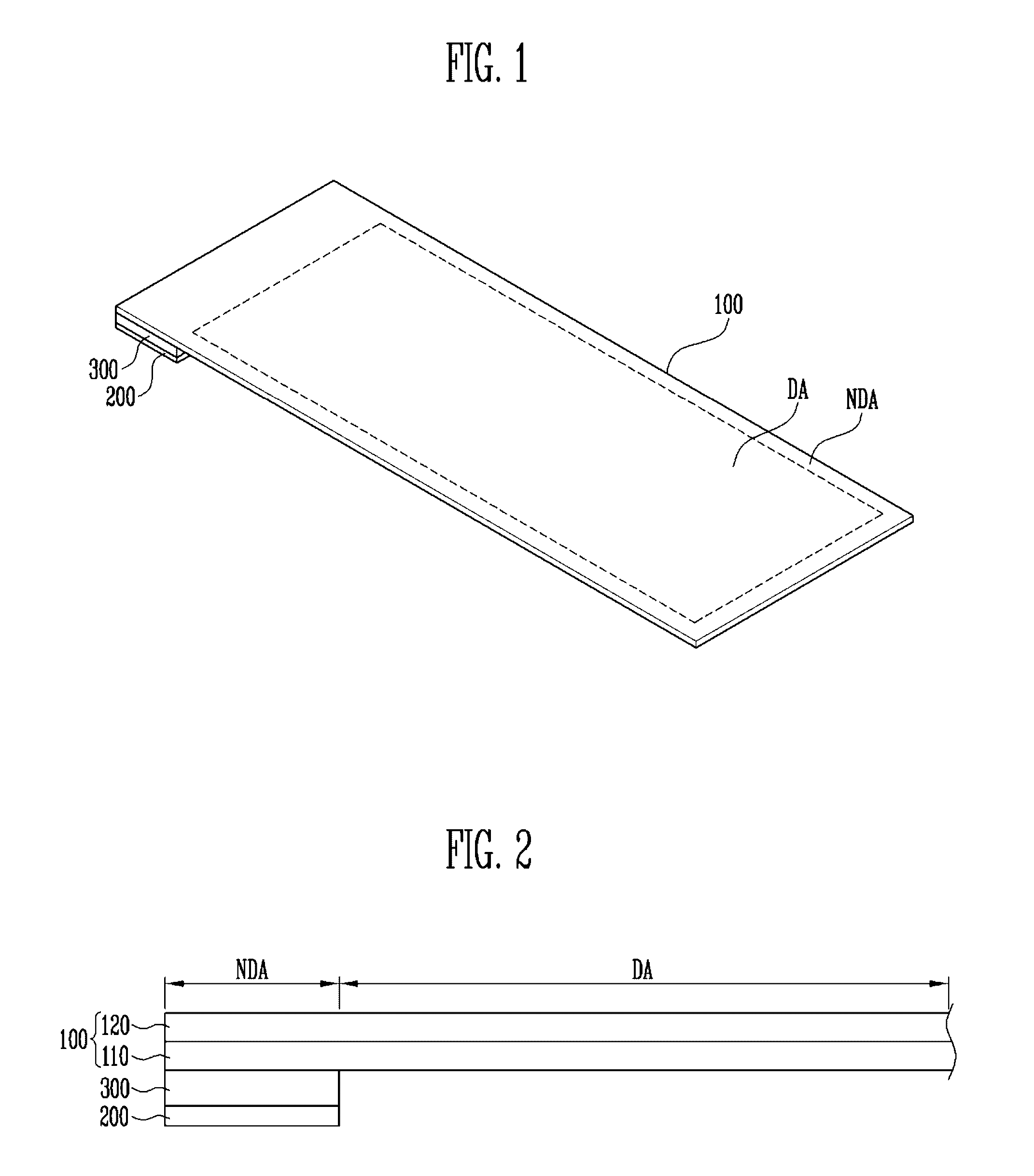
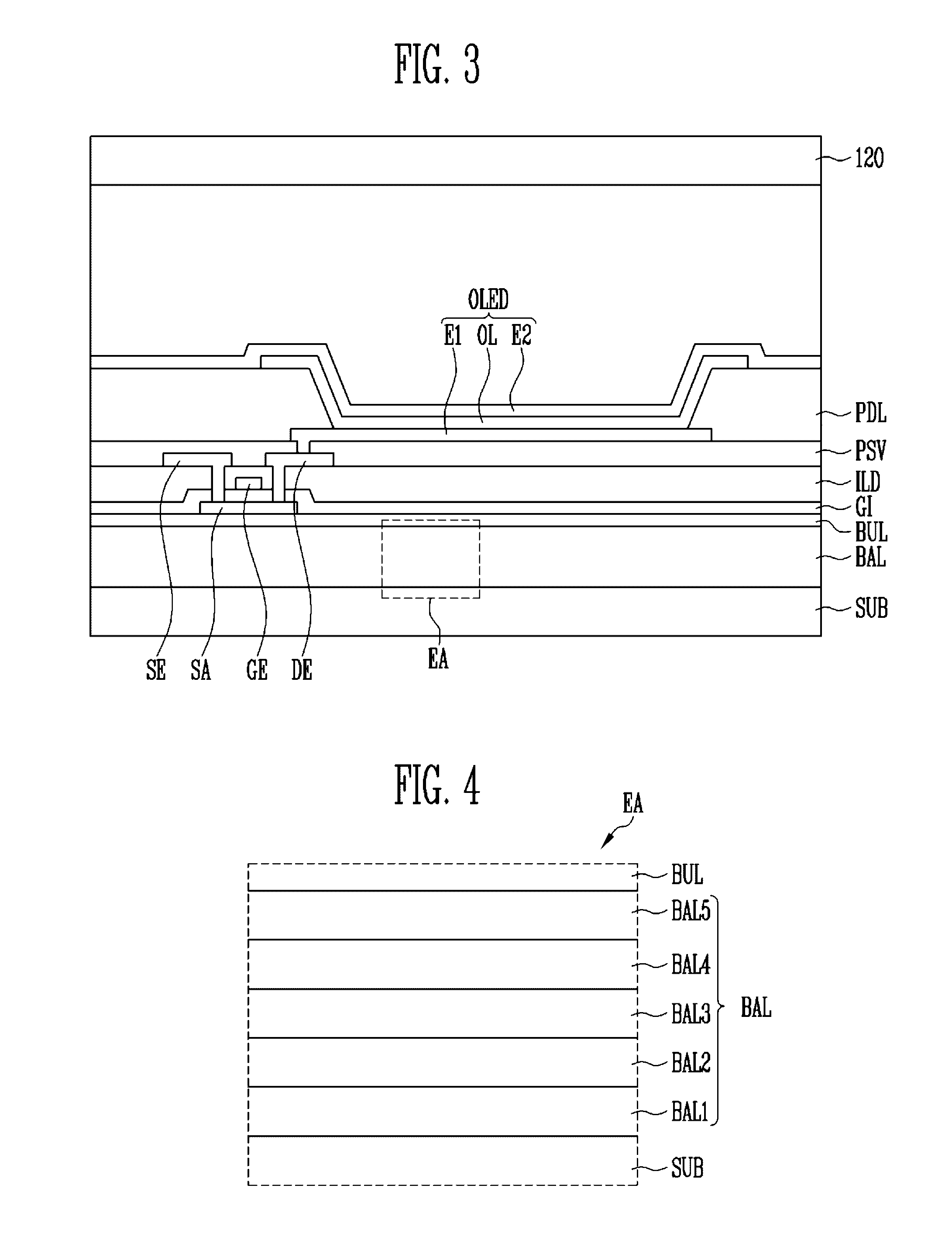
[0053]In the following detailed description, only some embodiments of the present invention have been shown and described, simply by way of illustration. As those skilled in the art would realize, the described embodiments may be modified in various different ways, all without departing from the spirit or scope of the present invention. Accordingly, the drawings and description are to be regarded as illustrative in nature and not restrictive. In addition, it will be understood that when an element or layer is referred to as being “on”, “connected to” or “coupled to” another element or layer, it can be directly on, connected or coupled to the other element or layer or intervening elements or layers may be present. In contrast, when an element is referred to as being “directly on,”“directly connected to” or “directly coupled to” another element or layer, there are no intervening elements or layers present. Like numbers refer to like elements throughout. As used herein, the term “and / o...


PUM


Abstract

A thin film transistor array panel device comprises: a base substrate; a barrier layer disposed over the base substrate and comprising a plurality of transparent material layers; and an array of thin film transistors disposed over the barrier layer. A difference between a refractive index of the barrier layer and a refractive index of the base substrate may be within about 6%. The transparent material layers may be arranged such that the transparent material layers having compressive residual stress and the transparent material layers having tensile residual stress are alternately stacked. Each of the transparent material layers may comprise silicon oxynitride (SiON).

Description

CROSS-REFERENCE TO RELATED APPLICATION[0001]This application claims priority to and the benefit of Korean Patent Application No. 10-2015-0061482, filed on Apr. 30, 2015, in the Korean Intellectual Property Office, the entire content of which is incorporated herein by reference in its entirety.BACKGROUND[0002]1. Field[0003]The present disclosure relates to a thin film transistor array panel and a display panel having the same.[0004]2. Description of the Related Art[0005]With development of the information-oriented society, various display panels such as an organic light emitting diode (OLED) display panel, a liquid crystal display (LCD) panel, an electrophoresis (EPD) panel and an electro-wetting display (EWD) panel are being used.[0006]In recent years, display devices have become thin and light weight, and highly mobile. Further, some display devices are even bendable or foldable. Such display devices may use a flexible substrate which includes a polymer resin instead of a glass sub...

Claims


Application Information

Patent Timeline
IPC IPC(8): H01L51/52H01L51/00
CPCH01L51/0097H01L2251/5338H01L27/1225H01L51/5256H01L27/1214H01L27/1218H01L29/78633H01L29/7869H01L29/78603H10K59/12H10K77/111H10K50/8445H10K2102/311H10K2101/00Y02E10/549H10K59/1213H01L29/7849
Inventor JUNG, SEUNG HOCHOI, CHAUN GIPARK, HYE YOUNGLEE, EUN YOUNGJEON, JOO HEECHO, EUN JEONGJEON, BO GEONCHUNG, YUNG BIN
Owner SAMSUNG DISPLAY CO LTD
Why Eureka
Try Eureka