Semiconductor display device and method of manufacturing the same

a display device and semiconductor technology, applied in the field of semiconductor display devices, can solve the problems of uneven display image, surface irregularities in the pixel electrode and the inequality thickness of the pixel electrode, and the inability to meet the needs of the user, and achieve the effect of limited film formation time and surface levelness

Inactive Publication Date: 2005-10-20
SEMICON ENERGY LAB CO LTD
View PDF81 Cites 36 Cited by
  • Summary
  • Abstract
  • Description
  • Claims
  • Application Information

AI Technical Summary

Benefits of technology

[0015] In view of the above problems, an object of the present invention is to provide a semiconductor display device with an interlayer insulating film in which surface levelness is ensured with a limited film formation time, heat treatment for removing moisture does not take long, and moisture in the interlayer insulating film is prevented from escaping into a film or electrode adjacent to the interlayer insulating film.
[0017] The present invention has been made in view of the above problems, and an object of the present invention is therefore to provide a technique of building thin film transistors in manufacturing a semiconductor display device that uses an organic resin film as an interlayer insulating film without allowing the threshold voltage to fluctuate among the thin film transistors, thereby improving the stability of the operation performance of the display device and enlarging the design margin in circuit design. Another object of the present invention is to improve the image quality of the display device.
[0020] What is important in this etching is to avoid exposure of the organic resin film in region where a wiring, a pixel electrode, or the like is formed not to be affected by moisture and by surface irregularities in a later step. The organic resin film may also be covered with an inorganic insulating film completely in the rest of the region.
[0021] In general, inorganic insulating films receive less etching damage in dry etching compared to organic resin films represented by acrylic resin films and accordingly the surface is roughened less. The pixel electrode or the like that is formed later is therefore saved from surface irregularities and uneven thickness, thereby preventing uneven display.
[0022] Covering the organic resin film with the nitrogen-containing inorganic insulating film that transmits less moisture compared to the organic resin does also prevents the organic resin film from releasing moisture contained within. Also this prevents the organic resin film from swelling with water in an alkaline aqueous solution which is used in development and thus saves heat treatment time for removal of moisture after development. Accordingly, moisture in the organic resin film is further prevented from escaping into a film or electrode adjacent to the organic resin film and the long-term reliability of the panel is enhanced. Moreover, in the case of a light emitting device which uses a light emitting element represented by an organic light emitting diode (OLED), it prevents degradation in luminance of the light emitting element due to moisture released from the organic resin film.
[0023] Covering the entire organic resin film with an inorganic insulating film to leave no region exposed further prevents the organic resin film from swelling with water in the alkaline aqueous solution which is used in development and thus save heat treatment time for removal of moisture after the development. Accordingly, moisture in the organic resin film is further prevented from escaping into a film or electrode adjacent to the organic resin film and the long-term reliability of the panel is enhanced.

Problems solved by technology

In addition to the wiring, if a pixel electrode is formed on the interlayer insulating film, the surface irregularities in the interlayer insulating film cause the surface irregularities in the pixel electrode and the inequality thickness of the pixel electrode.
This may result in unevenness in a displayed image.
Using an inorganic insulating film as the interlayer insulating film has a drawback because it takes time to form a film thick enough to level the surface using vapor phase growth method.
Wet etching is isotropic etching and therefore is not adaptable to wiring pattern miniaturization if it goes beyond 3 μm.
However, a problem of dry etching is that, when the conductive film on an organic resin film serving as the interlayer insulating film is treated by dry etching, the surface of the organic resin film is roughen.
With the surface of the organic resin film roughened, a flatness of the pixel electrode formed on the organic resin film is impaired and pixel display is accordingly affected.
There is a fear that the absorbed moisture corrodes over time the wiring that is in contact with the organic resin film and impairs the long-time reliability of the panel.

Method used


Image

  • Semiconductor display device and method of manufacturing the same
  • Semiconductor display device and method of manufacturing the same
  • Semiconductor display device and method of manufacturing the same

Examples


embodiment 1

[0167] In this embodiment, a manufacturing method of a light emitting device which is one of the semiconductor display devices of the present invention will be described. Note that, in this embodiment, a method of manufacturing a pixel portion and a storage capacitor included in a protective circuit at the same time will be described in detail.

[0168] First, as shown in FIG. 13A, a base film 5002 including an insulating film such as a silicon oxide film, a silicon nitride film, or a silicon oxynitride film is formed on a substrate 5001 including glass such as barium borosilicate glass or aluminoborosilicate glass represented by #7059 glass, #1737 glass, and the like of Coming Corporation. For example, a silicon oxynitride film 5002a manufactured from SiH4, NH3, and N2O is formed with a thickness of 10 to 200 nm (preferably 50 to 100 nm) by the plasma CVD method, and a silicon oxynitride hydrogenate film 5002b manufactured from SiH4 and N2O is likewise formed with a thickness of 50 t...

embodiment 2

[0226] In an active matrix semiconductor display device, a pixel portion has a plurality of pixels and a video signal is supplied through a signal line to a pixel that is chosen by a signal inputted to a scanning line. This embodiment gives a description on an example in which capacitor storage is used to reduce amplitude of noise of a signal inputted from a scanning line driving circuit to the scanning line.

[0227] First, the structure of a general active matrix liquid crystal display device is described. Although the description in this embodiment takes as an example a liquid crystal display device, the structure of the present invention is also applicable to other active matrix semiconductor display devices.

[0228]FIG. 18A is a block diagram of a semiconductor display device of the present invention. Denoted by 115 is a signal line driving circuit, 116, a scanning line driving circuit, and 120, a pixel portion. The signal line driving circuit 115 has a shift register circuit 115_...

embodiment 3

[0240] In this embodiment, a structure of a light emitting device having a sectional structure different from that of the light emitting device shown in Embodiment 1 will be described.

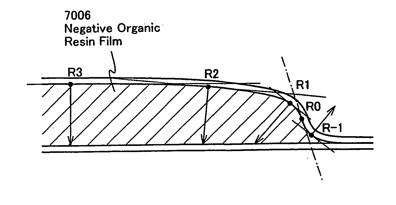
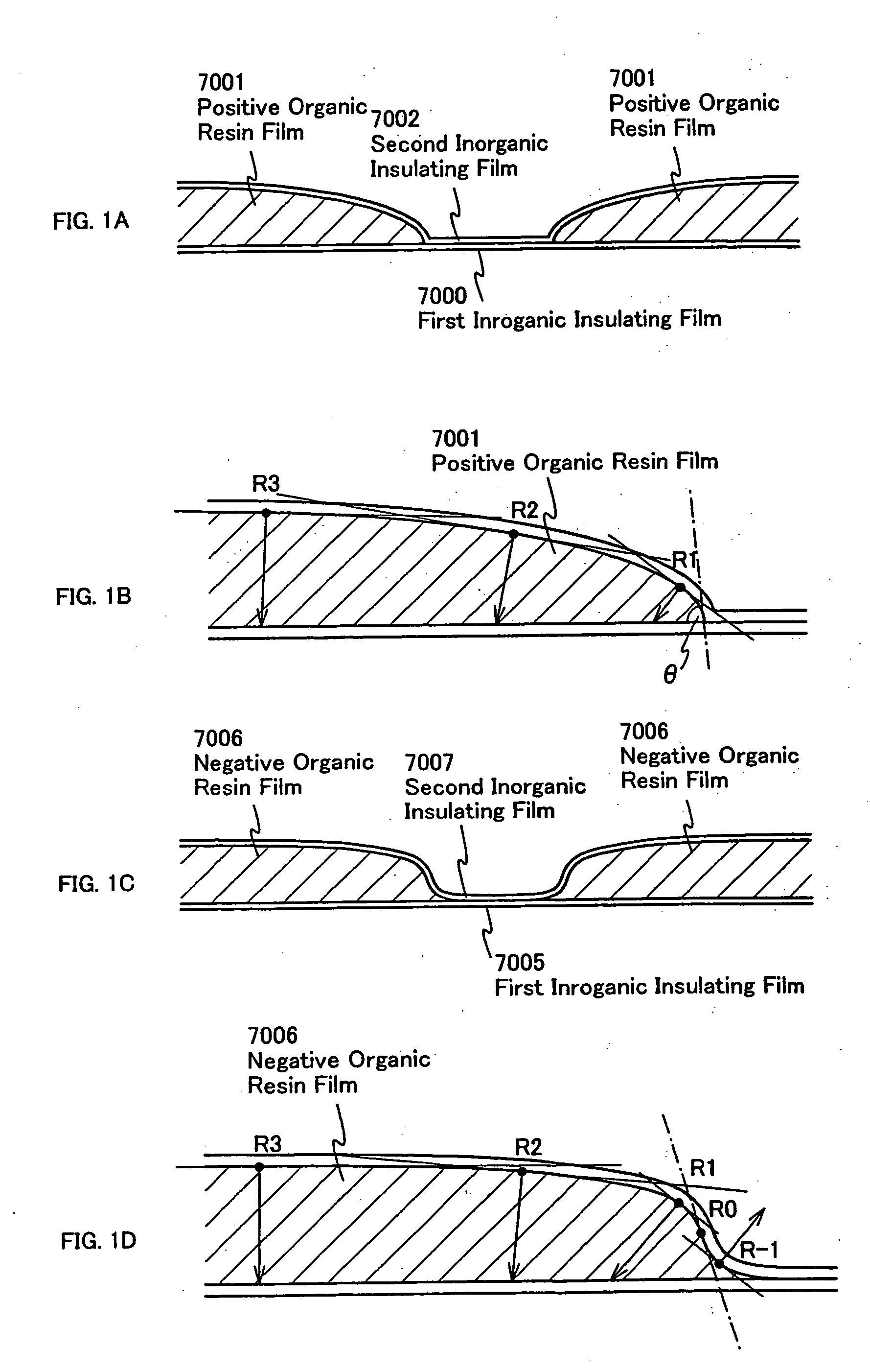
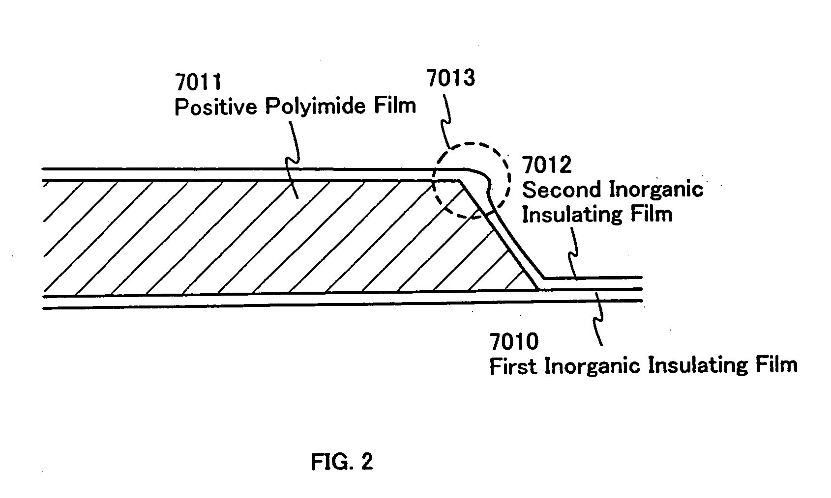
[0241] In a light emitting device shown in FIG. 21A, after forming a second inorganic insulating film 7500, a transparent conductive film is formed and patterned before forming a contact hole, whereby a pixel electrode 7501 is formed. Then, a gate insulating film 7502, a first inorganic insulating film 7503, and the second inorganic insulating film. 7500 are etched in an opening of an organic resin film 7504 to form the contact hole, and a wiring 7506 electrically connecting a TFT 7505 and the pixel electrode 7501 is formed.

[0242] In this way, by forming the pixel electrode 7501 before forming the wiring 7506, a process of polishing a surface of the pixel electrode before forming the wiring 7506 can be provided.

[0243] In a light emitting device shown in FIG. 21B, after forming a second inorganic ins...


PUM

PropertyMeasurementUnit
thicknessaaaaaaaaaa
radius ofaaaaaaaaaa
angleaaaaaaaaaa

Abstract

A semiconductor display device with an interlayer insulating film in which surface levelness is ensured with a limited film formation time, heat treatment for removing moisture does not take long, and moisture in the interlayer insulating film is prevented from escaping into a film or electrode adjacent to the interlayer insulating film. A TFT is formed and then a nitrogen-containing inorganic insulating film that transmits less moisture compared to organic resin film is formed so as to cover the TFT. Next, organic resin including photosensitive acrylic resin is applied and an opening is formed by partially exposing the organic resin film to light. The organic resin film where the opening is formed, is then. covered with a nitrogen-containing inorganic insulating film which transmits less moisture than organic resin film does. Thereafter, the gate insulating film and the two layers of the nitrogen-containing inorganic insulating films are partially etched away in the opening of the organic resin film to expose the active layer of the TFT.

Description

BACKGROUND OF THE INVENTION [0001] 1. Field of the Invention [0002] The present invention relates to a semiconductor display device which uses an organic resin film as an interlayer insulating film, and more specifically to a semiconductor display device structured which has a protective circuit formed in an input / output portion to protect internal circuits against breakage brought by high voltage load such as static electricity. [0003] 2. Description of the Related Art [0004] In recent years, a technique of forming a TFT on a substrate has greatly progressed, and its application and development for an active matrix semiconductor display device as one of the semiconductor devices have been advanced. In particular, since a TFT using a polycrystalline semiconductor film has higher field-effect mobility (also referred to as mobility) than a conventional TFT using an amorphous semiconductor film, it enables high-speed operation. It is therefore possible to control the pixel by the drive...

Claims


Application Information

Patent Timeline
Patent Type & Authority Applications(United States)
IPC IPC(8): G09F9/30H01L51/50H01L21/312H01L21/316H01L21/318H01L21/336H01L21/77H01L21/84H01L27/12H01L27/13H01L27/32H01L29/49H01L29/786
CPCH01L27/1244H01L27/1248H01L27/3244H01L29/4908H01L29/66757H01L29/66765H01L27/1255H01L29/78645H01L21/76804H01L21/76831H01L51/0037Y10S257/908Y10S257/906H01L29/78621G02F1/136204H10K59/12H10K85/1135
Inventor YAMAZAKI, SHUNPEIMURAKAMI, SATOSHIHAYAKAWA, MASAHIKOKATO, KIYOSHIOSAME, MITSUAKIHIROSUE, TAKASHIFUJIKAWA, SAISHI
Owner SEMICON ENERGY LAB CO LTD
Why Eureka
Try Eureka