

Waveguide Fabrication Method
- Summary
- Abstract
- Description
- Claims
- Application Information
AI Technical Summary
Benefits of technology
Problems solved by technology
Method used
Image

Examples
Embodiment Construction
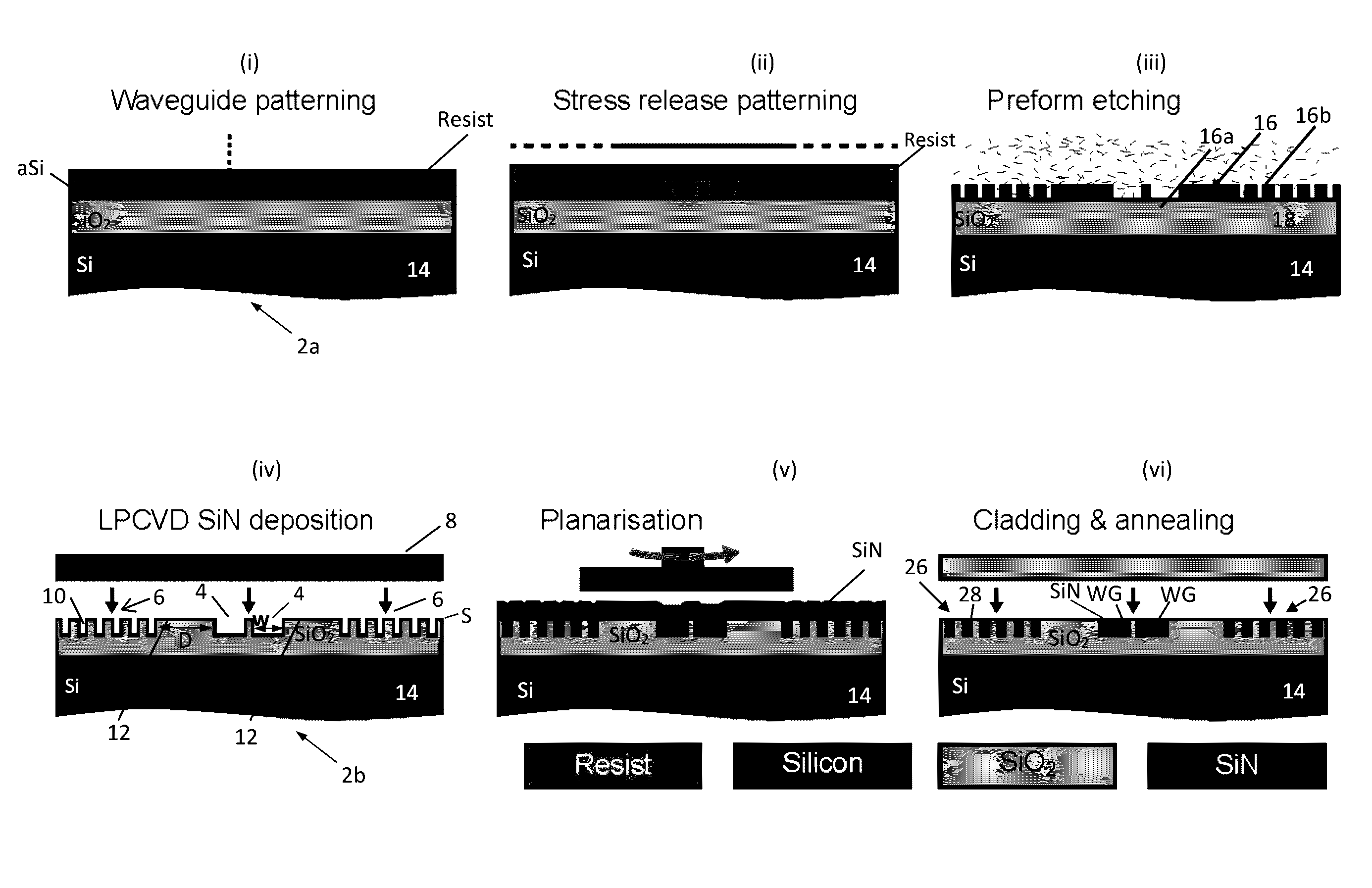
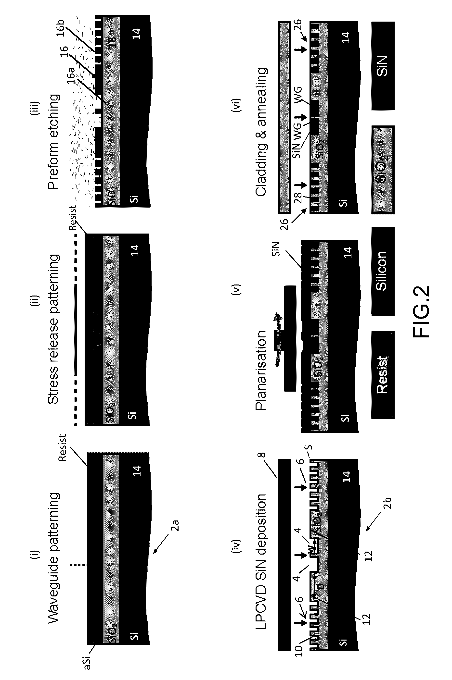
[0055]FIG. 2 shows one aspect of the present disclosure, depicting a waveguide fabrication method or photonic Damascene process for producing at least one waveguide or optical device. This waveguide fabrication method comprises providing a substrate 2b including at least one waveguide recess structure 4 and a stress release recess structure 6 for receiving a waveguide material 8.
[0056]The at least one waveguide recess structure 4 may define a substantially straight waveguide core extending across the substrate or resulting device or extending in the form of a spiral. The at least one waveguide recess structure 4 may define a resonator core, that is, a closed loop waveguide core for propagating electromagnetic energy repeatedly through the loop. The substrate 2b may alternatively include a first waveguide recess structure 4 defining a resonator core and a second waveguide recess structure 4 defining a coupling or bus waveguide core for inputting electromagnetic energy to the resonato...
PUM
 Abstract
Description
Claims
Application Information